8-Bit Move
Copies the content of one 8-bit register to another.
ddd = destination register (000-A, 001-B, 010-C, 011-D, 100-M1, 101-M2, 110-X, 111-Y)
sss = source register (000-A, 001-B, 010-C, 011-D, 100-M1, 101-M2, 110-X, 111-Y)Over the last five posts I’ve been building up the design of a set of cards so that the computer will be able to understand and perform the MOV-8, ALU and SETAB instructions. In this post I’m putting together the final piece of the jigsaw … the control card. This will take the instruction class from the decoder (which derives its result from the instruction register) along with the pulses generated by the sequencer to operate the various control lines of the computer as required.
There’s quite a bit of ground to cover here so I’ll visit the design of each individual instruction first in this post and then I can move on to bringing all the parts together on the new control card in my next post.
This instruction is the 8-bit move which selects the value in a given register on to the data bus and then loads another register with that value. The instruction has the code ‘MOV-8’ but you’ll often see the shorter ‘MV8’ used in the control design. The instruction takes the following form:
Copies the content of one 8-bit register to another.
ddd = destination register (000-A, 001-B, 010-C, 011-D, 100-M1, 101-M2, 110-X, 111-Y)
sss = source register (000-A, 001-B, 010-C, 011-D, 100-M1, 101-M2, 110-X, 111-Y)So for
example the instruction 00010011 would copy the value contained in the C
register to the D register. At the moment the M1, M2, X and Y registers aren’t
designed or built yet (they’ll be covered in a later post) so for now I’ll
only be designing and implementing MOV-8 for registers A, B, C and D.
Mapping the instruction out as a diagram we get the following:
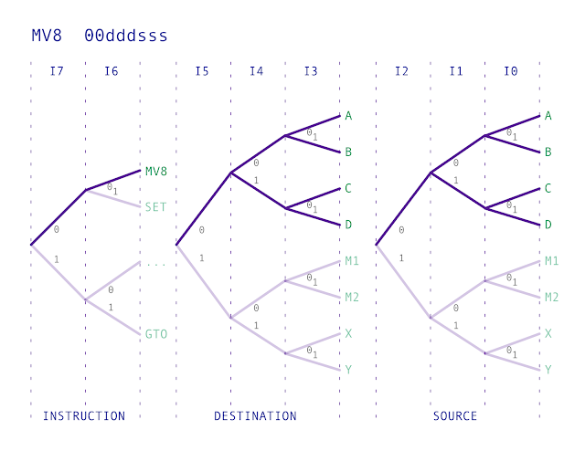
The decoder handles the first two bits of the instruction so it’s just a case of hooking a collection of relays together to handle the combinatorial logic of which register to select from / write to. In terms of timing we need the following:
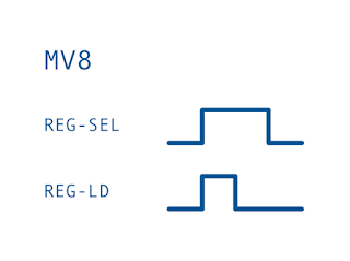
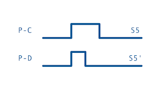
The first timing diagram shows how the source register is selected on to the data bus at the same time that the destination register is loaded but then the source register is held on for longer to ensure that the value has loaded before it’s taken off the bus. In terms of pulses P-C and P-D provide everything needed for this instruction.
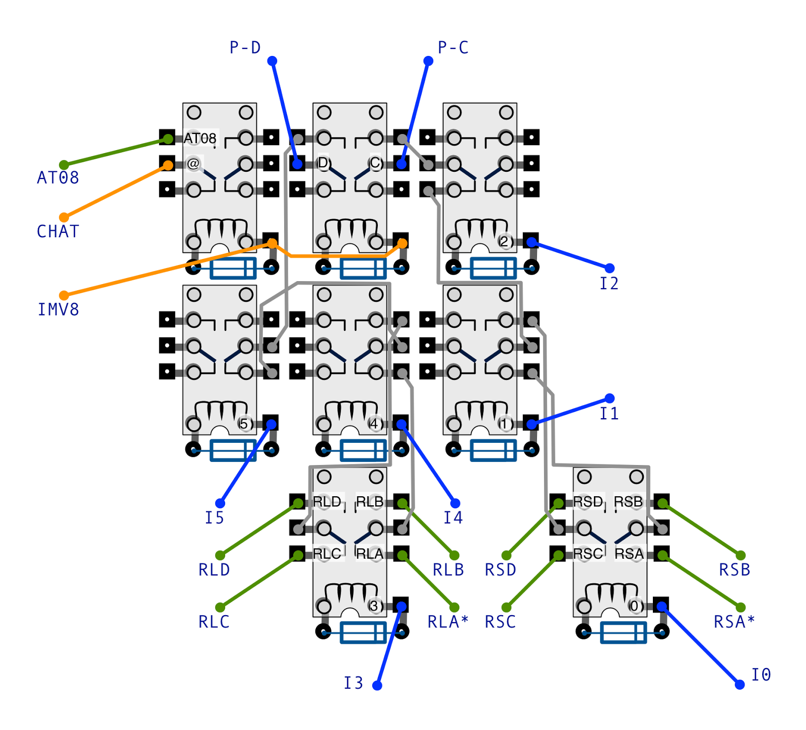
Taking the above three diagrams together the relay design is as follows:
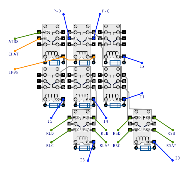
The relays are made up of three distinct areas of functionality:
One thing to note on the relay diagram above is the RLA and RSA lines (register load A and register select A respectively) are marked with a star. These two lines will need a diode placed shortly after the outputs as other parts of the control card will also produce this signal and the diode will ensure one part doesn’t back feed in to another. The other lines either aren’t used elsewhere on the control card or back feed wouldn’t cause any problems.
This instruction commands the ALU to perform a given operation on the value in register B (and optionally register C for operations with two inputs) placing the result on the data bus. The result is then placed in to either register A or D as required. The instruction takes the following form:
Performs an arithmetic or logic operation on the B (and optionally C) register(s).
  r = destination register (0-A, 1-D)
fff = function code (000-NOP, 001-ADD, 010-INC, 011-AND, 100-OR, 101-XOR, 110-NOT, 111-SHL)
So for example the instruction 10001011 would perform the logic AND of the values in register B and C and place the result in register D; the instruction 10000011 would increment the value in register B by 1 and place the result in register A.
Mapping the instruction out as a diagram we get the following:
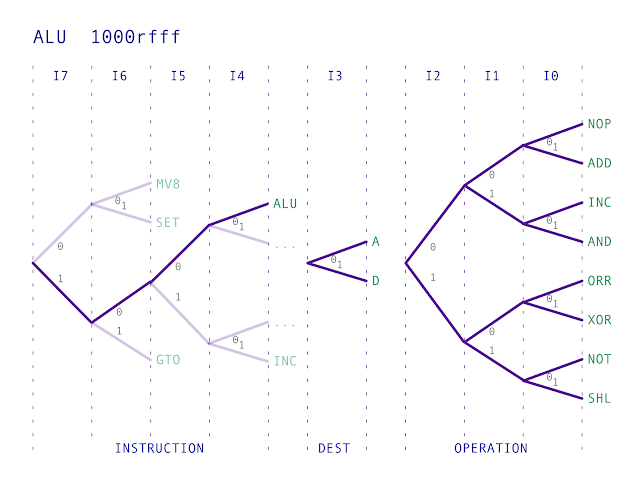
The decoder handles the first four bits of the instruction and in this case the ALU itself does most of the hard work (the last three bits are mapped directly to the ALU function code) so the only combinatorial logic needed in the control relays is which register to write to. In terms of timing we need the following:
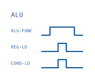
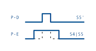
The first timing diagram shows how the ALU is commanded which places the result on to the data bus then whilst this value is present the destination register is loaded. At the same time the condition register is also loaded. The ALU is brought on early enough to let the value settle and long enough to ensure the registers have picked the value up. In terms of pulses P-D and P-E provide everything needed for this instruction.
Taking the above three diagrams together the relay design is as follows:
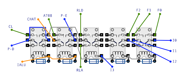
The relays are made up of four distinct areas of functionality:
As mentioned earlier, the control design for the ALU instruction is relatively straightforward as most of the hard work is done by the ALU card itself.
This instruction places a value contained within the instruction itself directly in to either the A or B register. The instruction has the code ‘SETAB’ but you’ll often see the shorter ‘SET’ used in the control design. The instruction takes the following form:
Loads a value between -16 and +15 in register A or B.
    r = destination register (0-A, 1-B)
ddddd = value (-16..15)
So for example the instruction 01101101 would load register B with a value of 00001101 (13); the instruction 01011111 would load register A with a value of 11111111 (-1). Effectively bit 4 of the instruction is repeated in bit 5, 6 and 7 of the register meaning that any value between -16 and 15 can be loaded up directly from the instruction.
Mapping the instruction out as a diagram we get the following:
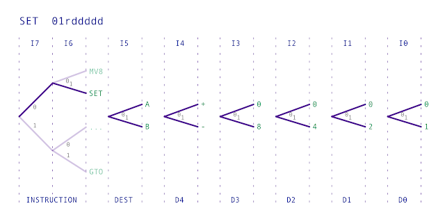
The decoder handles the first two bits of the instruction and with bits 0 through to 4 being gated directly to the data bus there’s only the combinatorial logic of which register to write to left to do. In terms of timing we need the following:
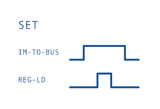

The first timing diagram shows how the value encoded within the instruction register is selected on to the data bus and then whilst that’s present the destination register is loaded. As before the incoming value is kept around long enough to ensure the destination register has had time to pick up the value. In terms of pulses P-D and P-E provide everything needed for this instruction.
Taking the above three diagrams together the relay design is as follows:
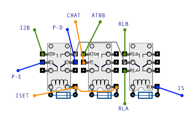
The relays are made up of three distinct areas of functionality:
One thing to note is that the I2B relays aren’t shown here and that’s because they’re not going on the control card. This is because they’ll need both the data and instruction buses together which can only be found on type ‘X’ cards. Fortunately there’s plenty of space free on the instruction register card (which is type ‘X’ as desired). The relays simply gate the values bit for bit but with bit 5 of the instruction duplicated on to bits 6, 7 and 8 of the data bus as mentioned earlier.
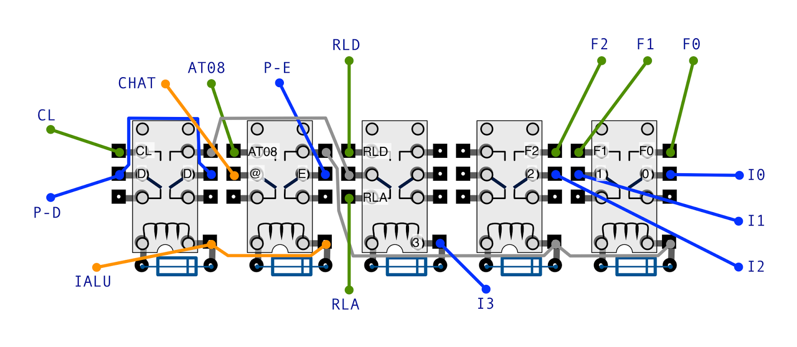
I’ve mentioned the CHAT signal repeatedly which is used by the control relays for each of the MOV-8, ALU and SETAB instructions. This tells the control relays when it’s a good time to announce the AT08 signal to the sequencer so it knows that it’s an 8-cycle instruction that’s being performed and that it should reset after 8 steps. The CHAT signal is raised on pulse D and then the resulting AT08 signal is latched in place by the sequencer until it needs it.
The relay that controls the CHAT signal is very simple:
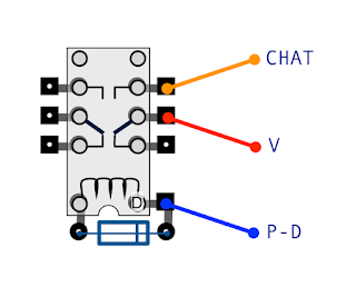
… when pulse D is active the power supply (V) is connected to the CHAT line.
That’s about it for this post. In my next post I’ll complete the design for the control card by placing the MOV-8, ALU, SETAB and CHAT relays and wire everything together. I’ll also cover the addition of the I2B relays on the existing instruction register card design.