In my last post I covered the design of the 8-cycle finite state machine (FSM). In this post I’ll now take the outputs from that FSM and combine them to produce the timing pulses that will be needed to perform the MOV-8, ALU and SETAB instructions. The sequencer and pulse distribution share a ‘double’ card and so I’ll also cover the resulting design when these two systems are combined.
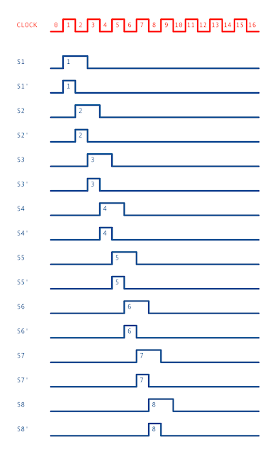
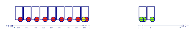
To quickly recap … the 8-cycle FSM will produce the following states given a clock signal as an input:
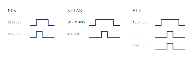
Producing the instruction timing pulses is very straightforward and is just a case of either taking the FSM states directly or combining them together so that we get the following:
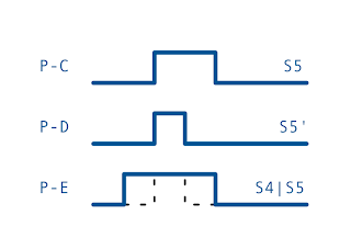
It really is as simple as that … all the hard work has been done in the design of the FSM. Where two or more FSM states are combined I’ll use diodes to stop any feedback upsetting the FSM - effectively the didoes act as a logic OR gate. Later on I’ll cover the control board design which will take these timing pulses and use them to operate the control lines thus:
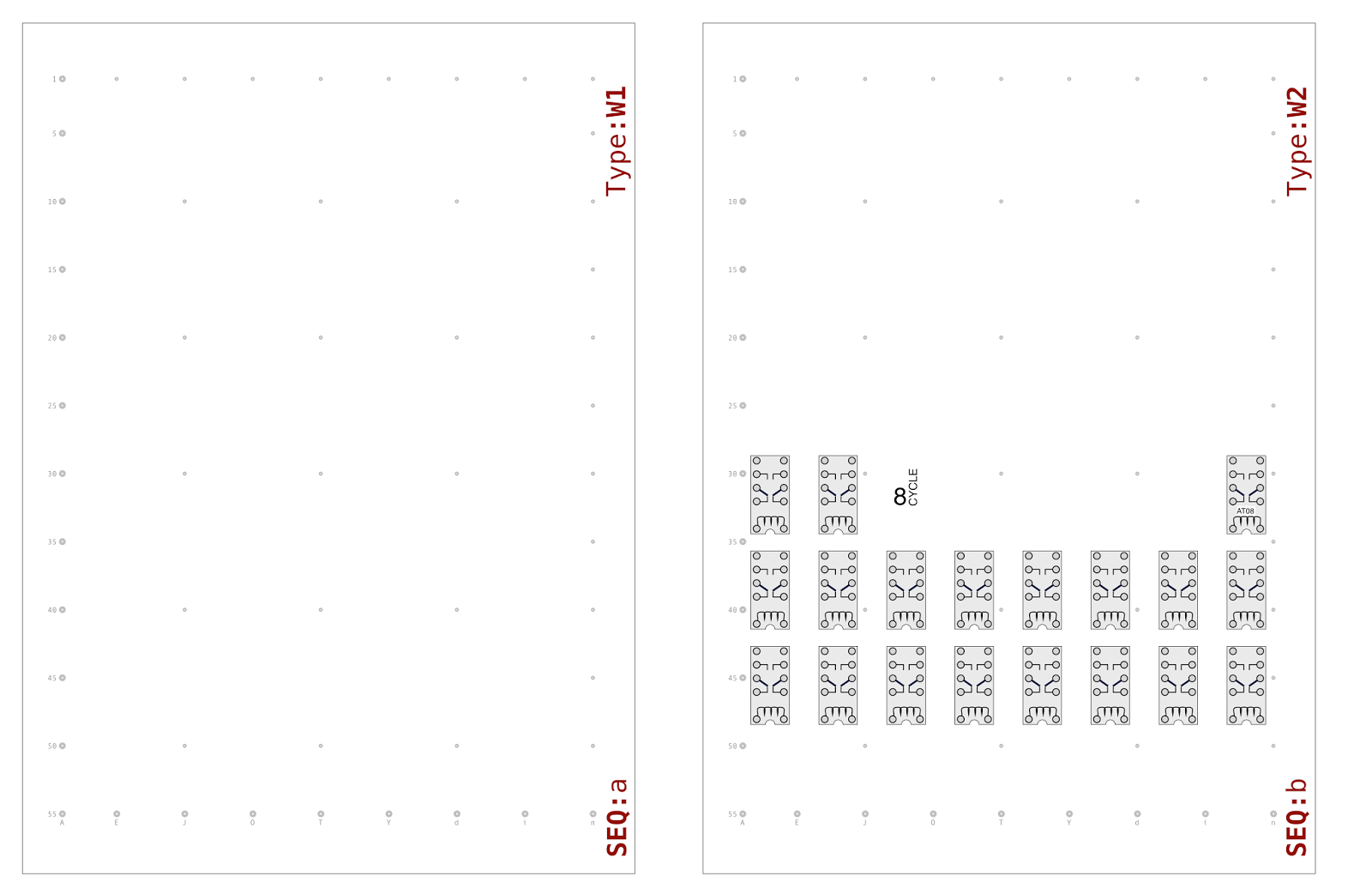
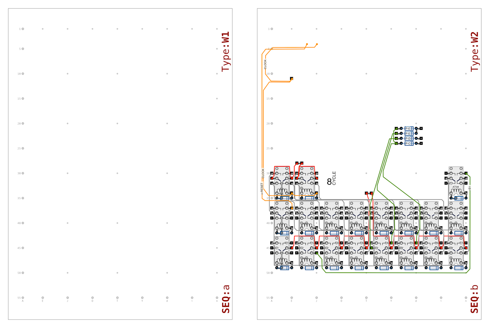
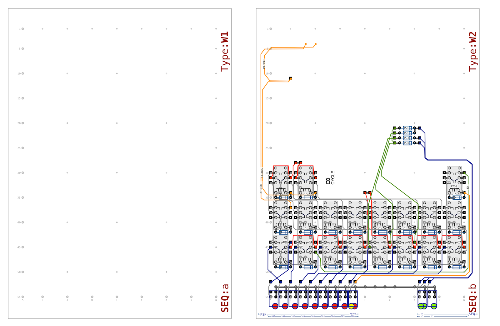
With the theory in hand we can take the sequencer design from my last post and wire up the timing pulses. I’ll start off with the basic relays on the usual 55 x 40 hole pad board:
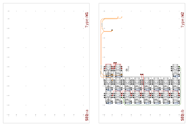
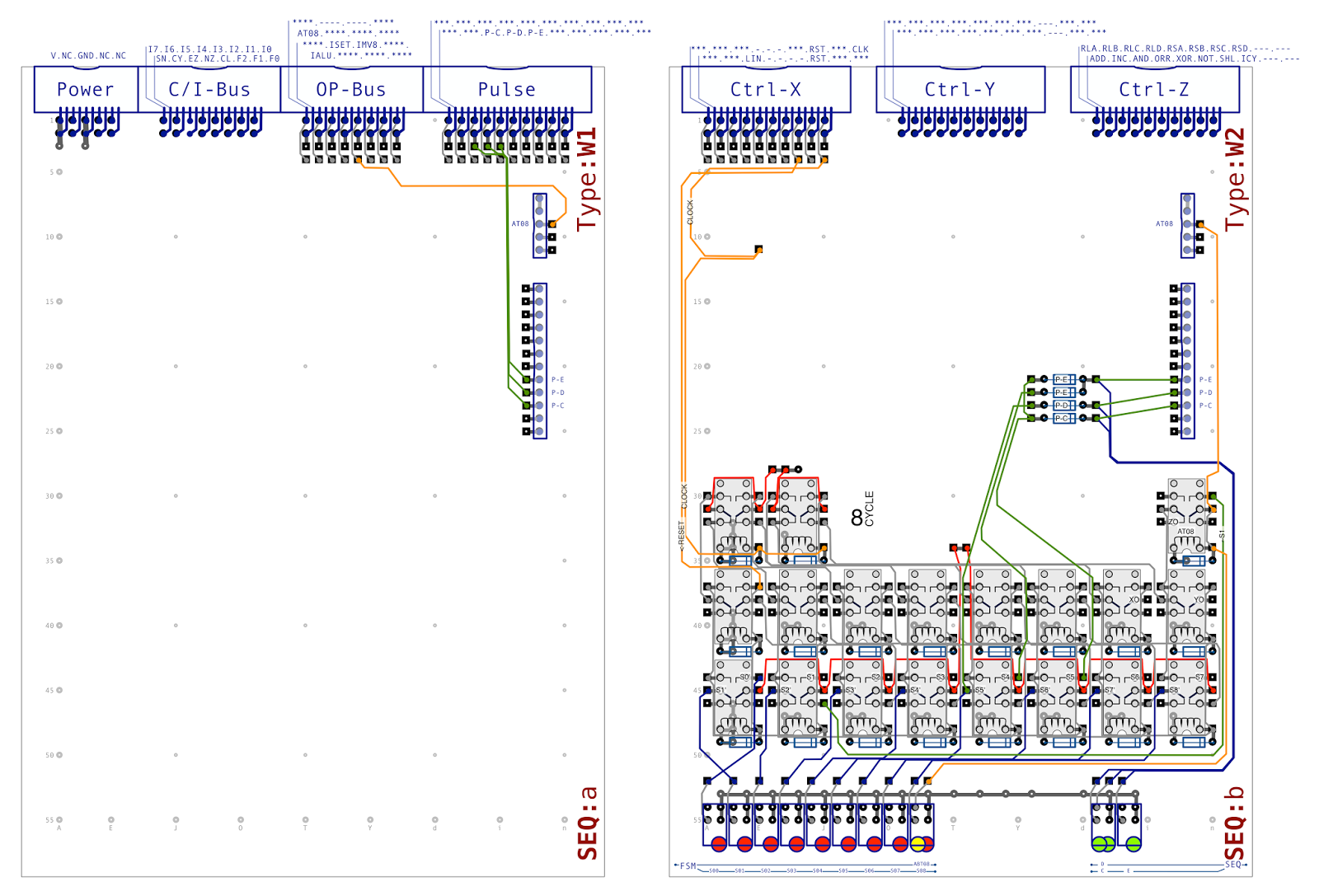
The only slight difference from the design in my last post is that the relays are now further down the second card than before. I ended up moving them around so that when additional functionality is added to the sequencer and pulse distribution things fit in better. If I add on all the internal wiring for the 8-cycle FSM we then get the following:
The FSM takes the clock and reset signal as inputs (shown as the yellow lines above). The FSM outputs are labelled on the lowest row of relays with the one clock ’tick’ Sx’ state outputs to the left of each relay and the two clock ’tick’ Sx outputs to the right. To recap again from my last post … the top left pair of relays take the clock signal and repeat out for when the clock is both high and low — this drives the FSM ring counter on the two rows of relays below. The top right relay is the 8-cycle abort relay — this is used to restart the FSM when the 8th state is reached. Eventually the FSM will be extended to allow for longer cycle instructions and for these the 8-cycle abort relay will be deactivated allowing the FSM to continue on.
With the FSM in place I can now tap the state outputs to create the timing pulses:
I’ve decided that even where multiple FSM states don’t need to be combined, that is, where a single state is mapped directly to a timing pulse, that I’ll still use a diode to stop any back-feed.
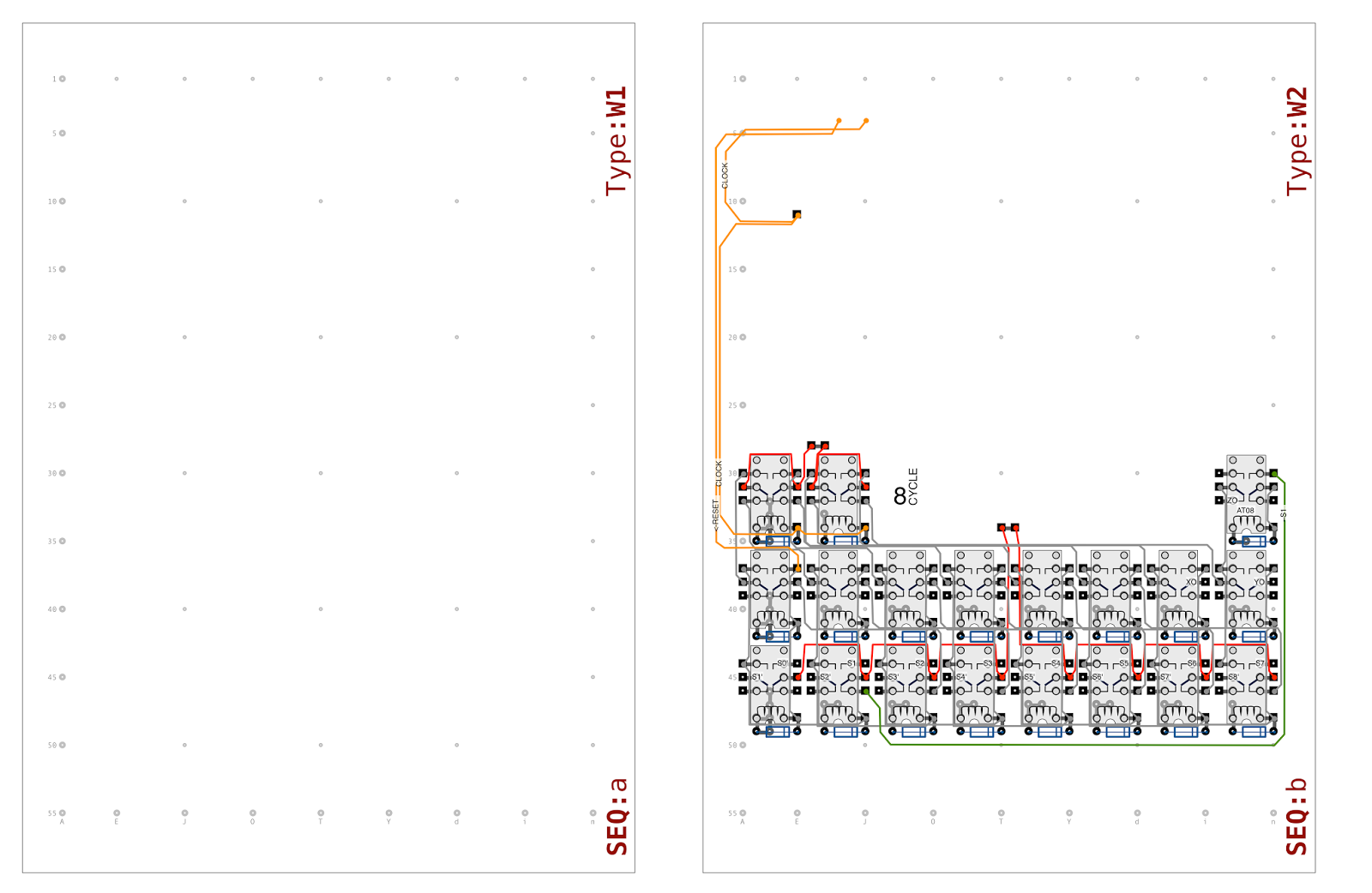
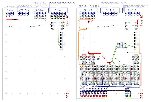
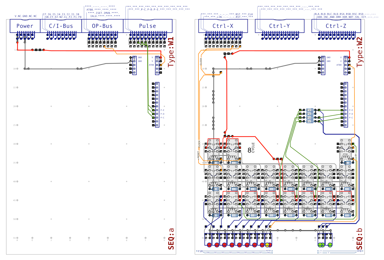
As with every card designed to date I’ll want to add the all important ‘flashing lights’ so I can see what the card is up to. As there’s nothing on the left hand ‘W1’ card it’s only the ‘W2’ card that’ll need indicators on it … for now at least. Here’s what they look like:
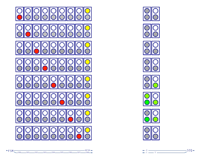
On the left are the outputs from the FSM. Each of the Sx’ outputs are shown (although they’re labeled as though they are the Sx outputs). The Sx’ output is used so that each lights up in turn rather than having two light up together as would be the case if the Sx states we used. All the LEDs are the usual 12V 3mm LEDs used on every other card so far and are placed in a two row holder. Note that the first 8 holders will have the top hole vacant with only the last holder having the yellow ‘ABT08’ LED present — this will make more sense aesthetically when longer FSM cycles are added. At the far right are the final timing pulses (labelled SEQ here for SEQuencer output). Again the LED holders are double row and is generally laid out so that the longer pulses are on the bottom row with the shorter ones on top.
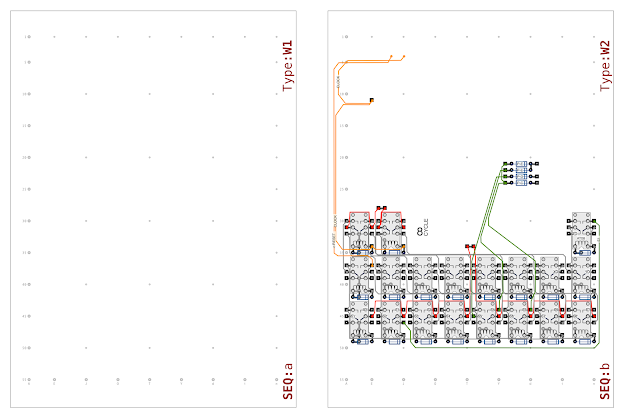
Here is a diagram of how the indicators would look when stepping through the states of the 8-cycle FSM:
With the indicators added to the design so far we get the following:
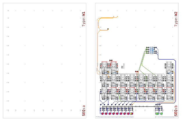
The
next job is to add to the connectors so that the cards can talk to the rest of
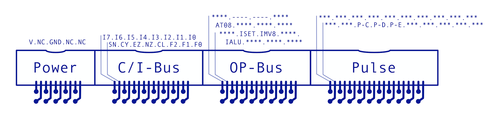
the computer. These are the connectors we’ll need, firstly for the ‘W1’ card
on the left followed by the ‘W2’ card on the right:
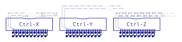
These are the usual right angle boxed headers used on previous cards and as before lines marked ‘’ (or ‘*’) are reserved for future use with lines marked ‘—’ (or variants of) are unused.
The lines on the W1 connectors are as follows:
- C/I-Bus (Control Bus + Instruction Bus)
- I0-I7 … 8-bit Instruction Bus
- F0-F2 … 3-bit ALU Function Code
- CL … Condition Register Load
- SN/CY/EZ/NZ … Condition Flags (Sign, Carry, Zero, Non-Zero)
- OP-Bus (Operation Bus)
- AT08 … Abort-8 Signal (Tells the FSM to reset at stage 8)
- ISET/IMV8/IALU … Instruction Class (SETAB, MOV-8, ALU)
- Pulse Bus
- P-C/P-D/P-E … Timing pulses C, D and E
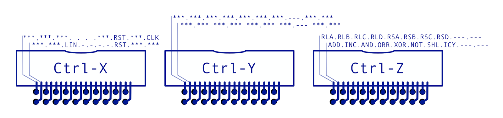
On the W2 connectors the lines are as follows:
- Ctrl-X (Control Line Bus)
- LIN … Instruction Register Load
- RES … Sequencer Reset
- CLK … Clock Signal
- Ctrl-Y (Control Line Bus)
- Ctrl-Z (Control Line Bus)
- RLA/RLB/RLC/RLD … Register Load A, B, C, and D
- RSA/RSB/RSC/RSD … Register Select A, B, C and D
- ADD/INC/AND/ORR/XOR/NOT/SHL/ICY … Internal ALU control lines

As always should you wish to take a much closer look at this design (and to be fair, this is one of the more ‘busier’ cards visually so a close look is advised) you can find the above here in PDF format.
So, I’m actually quite a good way through designing the cards that will allow the computer to operate a full instruction given an opcode. I’ve got the designs all done for the instruction register, instruction decoder and now the sequencer (including FSM and pulse distribution). Next up comes the control card … this will take the decoded instruction along with the timing pulses generated by the FSM and use both to operate the various control lines of the computer at the right time as needed. Last job after that will be to add a few more items to the front switch control card and the two display cards to reflect the functionality I’ve added in this batch of cards and then it’ll be on to construction.
Once I’ve built all the cards above I’ll be able to manually load an instruction into the register and then watch it be executed as I manually operate the clock line. The good news from there is that I only need to add the clock card to get to the next level towards having a fully working computer.