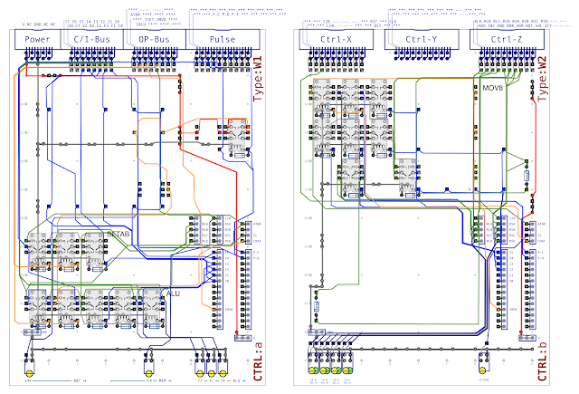
In part one of this two part post I introduced the design of the control relays for each of the MOV-8, ALU and SETAB instructions. With these in hand I can now move on to placing these on the control cards and wire everything together. That’s ‘cards’ rather than ‘card’ as the control relays will be spread over two cards just like the sequencer relays are. This is partly because there’s more relays than would fit on a single card but mainly because access to a wider range of busses is needed.
Getting stuck in, here is all the relays laid out across the two new control cards:
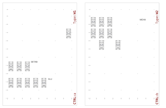
On the left hand card there is the CHAT relay floating at the top right then down from there are the three SETAB relays and below that the five ALU relays. On the right hand card there is the eight MOV-8 relays. As with the sequencer card there will be more relays added to these cards as further instructions are added.
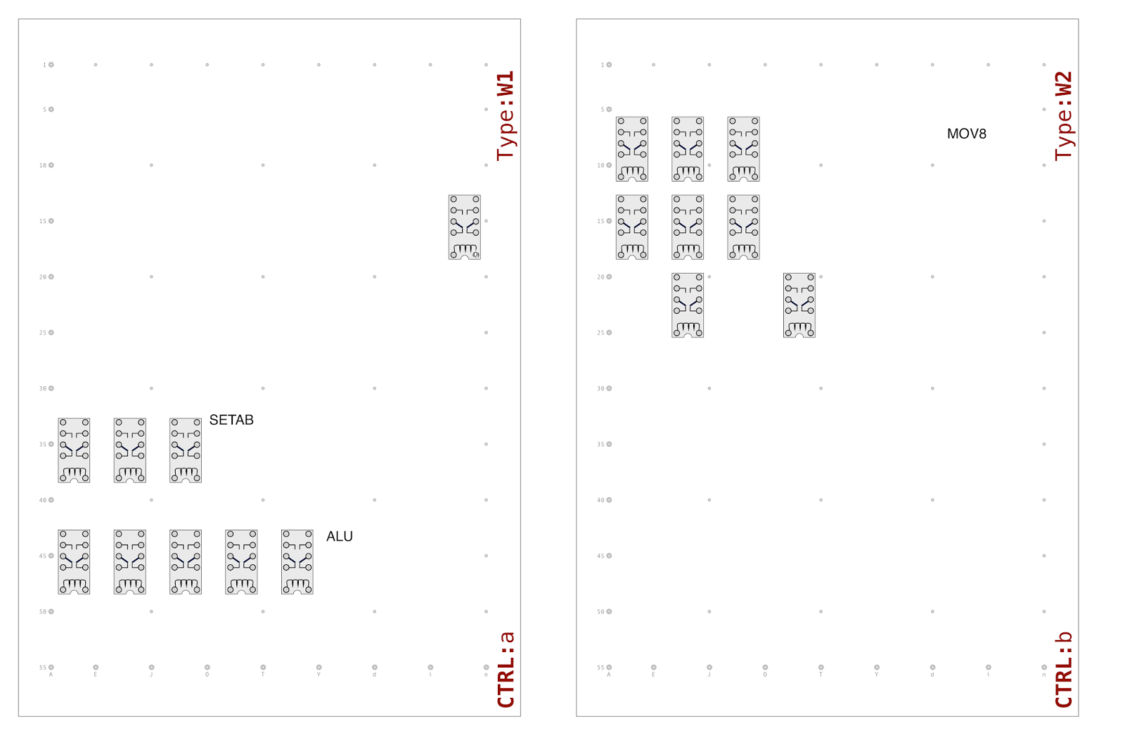
Adding in the wiring posts, internal links and diodes gives the following:
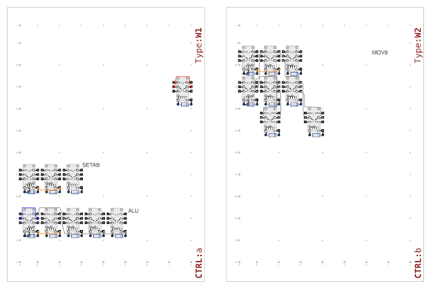
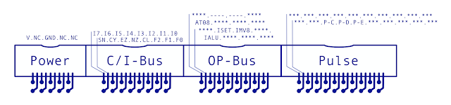
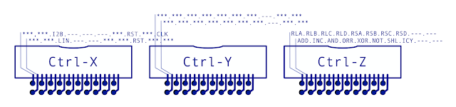
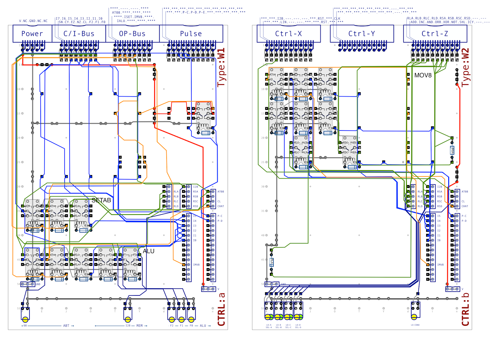
The next job is to add the connectors so the relays can be wired up to their inputs and outputs as required. As these cards are W1 and W2 types they use the same connectors as the respective W1 and W2 cards of the sequencer. These are the connectors we’ll need, firstly for the ‘W1’ card on the left followed by the ‘W2’ card on the right:
These are the usual right angle boxed headers used on previous cards and as before lines marked ‘***’ (or ‘****’) are reserved for future use with lines marked ‘---’ (or variants of) are unused.
The lines on the W1 connectors are as follows:
- C/I-Bus (Control Bus + Instruction Bus)
- I0-I7 … 8-bit Instruction Bus
- F0-F2 … 3-bit ALU Function Code
- CL … Condition Register Load
- SN/CY/EZ/NZ … Condition Flags (Sign, Carry, Zero, Non-Zero)
- OP-Bus (Operation Bus)
- AT08 … Abort-8 Signal (Tells the FSM to reset at stage 8)
- ISET/IMV8/IALU … Instruction Class (SETAB, MOV-8, ALU)
- Pulse Bus
- P-C/P-D/P-E … Timing pulses C, D and E
On the W2 connectors the lines are as follows:
- Ctrl-X (Control Line Bus)
- I2B … Immediate To Bus (Places the value encoded in a SETAB instruction on to the data bus)
- LIN … Instruction Register Load
- RES … Sequencer Reset
- CLK … Clock Signal
- Ctrl-Y (Control Line Bus)
- Ctrl-Z (Control Line Bus)
- RLA/RLB/RLC/RLD … Register Load A, B, C, and D
- RSA/RSB/RSC/RSD … Register Select A, B, C and D
- ADD/INC/AND/ORR/XOR/NOT/SHL/ICY … Internal ALU control lines
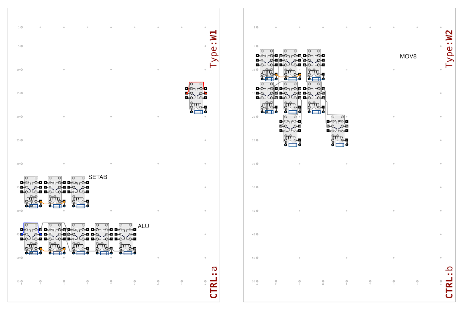
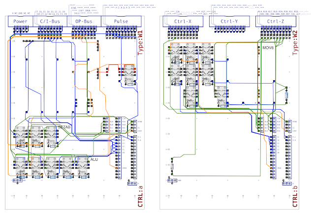
As with the sequencer cards the W2 card will need some lines on the W1 connectors and vice-versa. The solution is the same where by interconnections are made between the two cards so that they act as one larger card. With the primary card connectors, internal interconnects and other connector wiring added to the design we get the following:
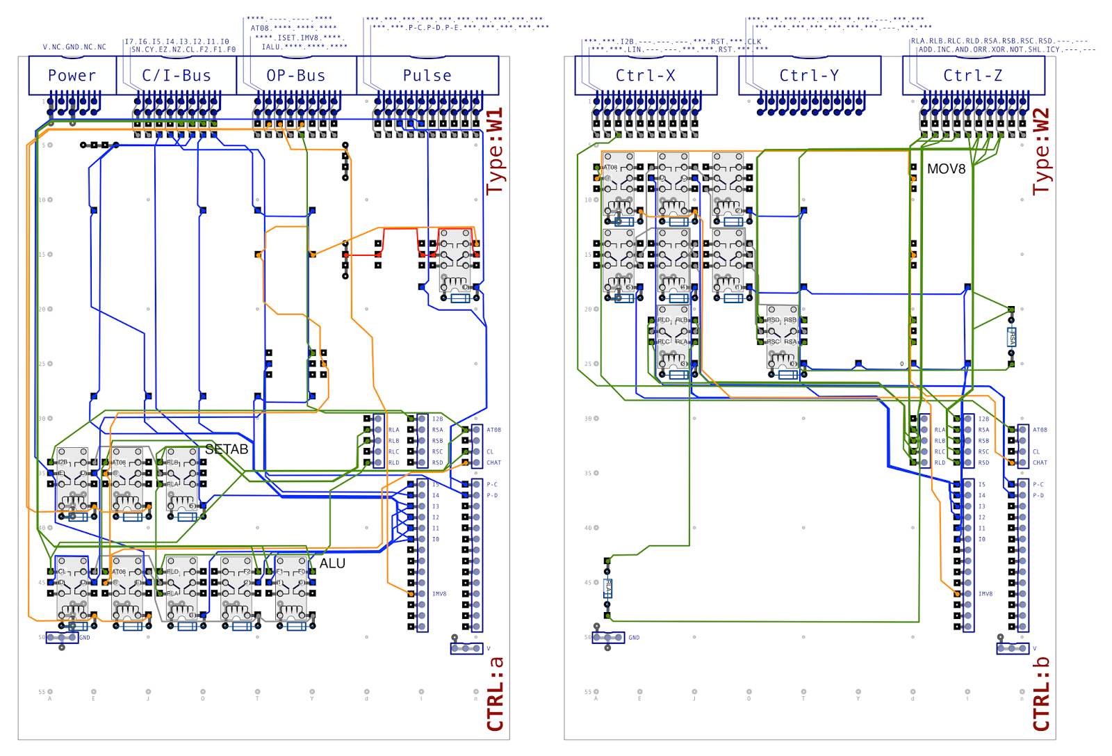
There’s a couple of things that probably warrant further explanation on the above diagram. Firstly you can see that some of the lines going to and from the instruction relays don’t run a direct route and stop off at various points. This is where future instruction relays will be placed and they’ll also be interested in the same lines hence the diagram above shows where the wires will actually go when the cards are constructed. There’s also an appearance of the additional diodes in the select register A and load register A lines on the second card. These prevent feed back on these lines as mentioned in my last post but the position of the diodes is again placed to work around future relays.
As with other cards I’ll want a line of LEDs down the front of each card to display what’s going on within. Firstly for the W1 card on the left followed by the W2 card on the right we have:
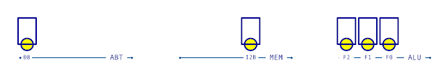
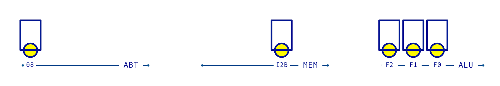

The W1 card LEDs show the ABT08 line status and that of the I2B line raised by the SETAB instruction. This is then followed by the three bits of the ALU function code raised by the ALU instruction. The W2 card LEDs show the load and select lines of registers A through to D variously operated by all three instructions. This is the followed by the condition register load line raised by the ALU instruction.
Adding the indicators above to the cards along with the power supply lines (which are soldered to the back of the card) we arrive at the final design as follows:
As always should you wish to take a much closer look at this design you can find the above here in PDF format.
Before I wrap up this post there’s one extra bit to sort out. The SETAB instruction needs a set of relays to gate the lower bits of the instruction bus on to the data bus. These relays can’t be placed on the control cards as both the instruction and data busses are required so instead they can live on the instruction register. With these added I2B relays the instruction register design now looks like this:
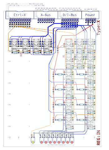
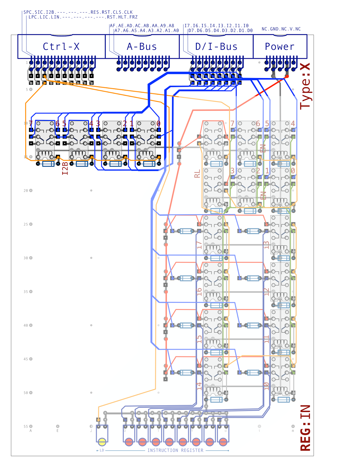
In the above diagram I’ve faded out the existing instruction register relays and wiring to highlight the new I2B relays added. There’s also the full version of the revised instruction register design available as here in PDF format.
… and that’s the control card design complete for the MOV-8, ALU and SETAB instructions. This now joins the designs for the instruction register, instruction decoder and sequencer (including FSM and pulse distribution). The last job now is to add a few more items to the front switch control card and the two display cards to reflect the functionality I’ve added in this batch of cards and then it’ll be on to construction. Once I’ve built all the cards above I’ll be able to manually load an instruction into the register and then watch it be executed as I manually operate the clock line. The good news from there is that I only need to add the clock card to get to the next level towards having a fully working computer.