I’ve almost got everything I need now to get my relay computer to do branching. The hard work of designing and constructing
the sequencer and controller units is complete and both units can perform a GOTO operation. The only problem now is the
decoder card doesn’t understand what a GOTO instruction looks like and so can’t tell the controller unit to perform a GOTO.
That’s easily fixed though as the decoder is one of the simplest cards in my computer.
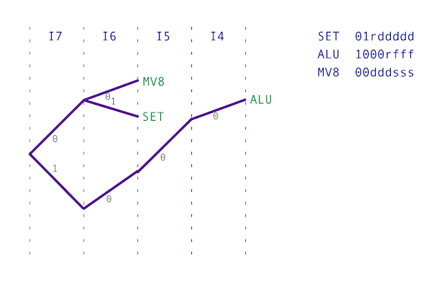
So far the existing decoder can understand ALU, MOV8 and SETAB instruction classes. Mapped out as a tree diagram it looks like
this:
Given the GOTO instruction …
Branch/Call & 16-bit Load Immediate
GOTO24
11dscznx
hhhhhhhh
llllllll
Branches to a given address if stated condition register flag(s) is set. Address of next instruction can optionally be saved in XY register. M register can also be loaded with 16-bit value (without jump).
d = destination register (0-M, 1-J)
s = 1 = load PC if sign bit is set (if negative); 0 = ignore sign bit
c = 1 = load PC if carry bit is set (if carry); 0 = ignore carry bit
z = 1 = load PC if zero bit set (if result is zero); 0 = ignore if zero bit set
n = 1 = load PC if zero bit clear (if result is not zero); 0 = ignore if zero bit clear
x = 1 = copy PC to XY; 0 = no copy
hhhhhhhh = address high byte (to set in M2/J2)
llllllll = address low byte (to set in M1/J1)
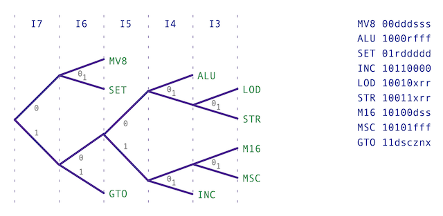
… we can see that it will always start with ‘11’ and so updating the tree diagram is simple enough. However, as I want
to design and build this card completely I’m going to add the other instruction classes I know my computer will be needing. I
won’t cover these in too much detail yet (I’ll save those for another time) but suffice to say that the controller cards are
already capable of performing these instruction classes - they’ll just need more relays soldering into the existing PCB.
Anyho, here’s the complete decoder tree diagram:
You can perhaps see that designing these opcodes requires quite a bit of thought. The MOV8 instruction, for example, starts
with a ‘00’ because we want to reserve the following six bits as parameters to that instruction type - same goes for the GOTO
instruction. However that means we’ve already used up half of the opcode permutations. The SETAB instruction (starting with
‘01’) polishes off another quarter as it also needs six bits for its parameters.
So, that leaves us with a quarter of the possible opcode permutations for everything else. Fortunately most of the remaining
instructions aren’t quite as parameter hungry … or rather, they’ve been designed that way. This is why sometimes an
instruction is limited in what it can do. For example, SETAB can only load register A or B because otherwise we’d need to find
an extra bit in the instruction at the cost of another instruction.
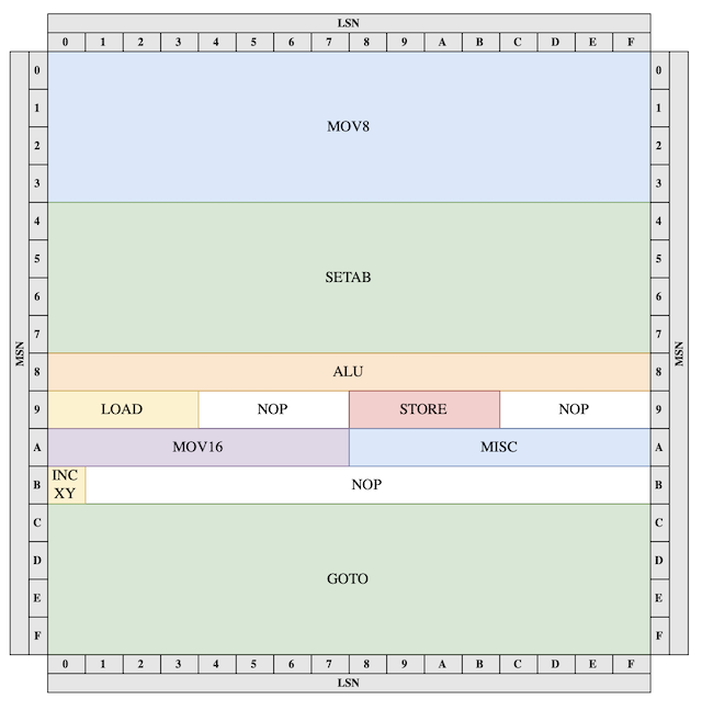
Another way of visualising the possible permutations of instructions is via a map which shows how much ‘space’ each
instruction class takes up what’s available:
You can see that we have several blank sections marked ‘NOP’ which stands for ‘No Operation’. These are areas where there’s
potential space for adding more instruction types in the future.
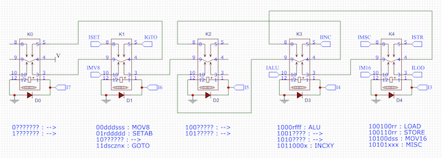
Right, let’s move on to designing the relay logic for the decoder and all we need to do is wire out the tree map you see
above:
To that we just add the standard W1 backplane connectors which will bring in power, control/instruction bus, operation bus and the pulse bus. For this card the instruction bus is our input and the operation bus is the output. Finally the card needs
a set of LEDs on the front to display the currently decoded instruction class. This all results in the final schematic
which you can find here in PDF format.
For the PCB design we follow the usual steps: place components that have to be in a certain location first; place other
components in rough logical groups; lay tracks; build ground/power planes; add text labels etc. Being as this card is so
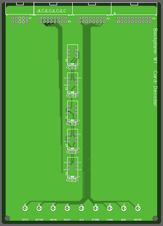
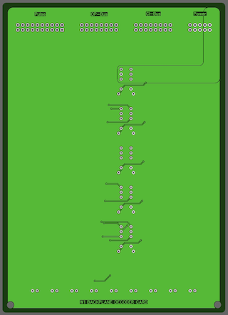
straightforward let’s skip to the finished design - here’s a ‘realistic’ image of the final board design:
Decoder Card (front and rear)
If you’d like to take a closer look at these you can find the full colour previews in
PDF format here and another version here
which seperates the layers out.
That’s the decoder design fully complete and so all I’ve got to do now is solder it up and the computer should be ready
to perform its very first branching program.