In my last couple of posts I finalised the controller schematic designs for the ALU, SETAB, MOV8 and GOTO class of instructions. Now it’s time to bring all those schematics together and design the two controller PCBs. As with the sequencer, the controller is spread over two interconnected cards and I’ll need to decide what’s going on the upper card and what will go on the lower card.
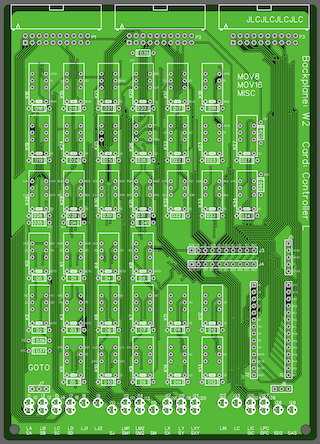
It’s also worth mentioning at this point that the schematics and PCB designs I’m about to share will have some instruction classes laid out that I haven’t covered yet in this blog. This is because you can’t ‘half design’ a PCB. I’ll cover these new instructions in more detail in the future but suffice to say that they’ll definitely be needed. In choosing what will go on which card I follow a similar rule to what I did on the sequencer and go by the number of relays required in each functional group. In the end I’ve gone for putting GOTO and MOV8/MOV16/MISC on the lower card and everything else on the upper card.
Schematic wise then it’s just a case of splitting things out and working out which signals will need to be passed between the cards. Let’s cut to the chase then … you can find the consolidated upper controller schematic here and the lower controller schematic here (both in PDF format). In both cases the card is largely defined by the backplane connectors it uses … W1 for the upper card (made up of address, operation and pulse busses) and W2 for the lower card (made up of Control X, Y and Z busses).
For the PCB design we follow the same basic steps as before for the sequencer: place components that have to be in a certain location first; place other components in rough logical groups; lay tracks; build ground/power planes; add text labels etc. Again, we’ll also need to pass additional signals between the cards via an ‘interconnect’. Let’s start then with the backplane connectors as these pre-exist on the W backplane and have to be in a certain location:
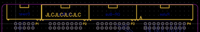
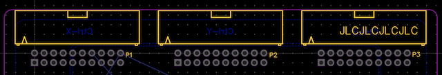
As before with the sequencer cards the ‘JLCJLCJLCJLC’ text in the top right corner is to let my PCB manufacture know where I’d like them to put their identification code so they can find my PCB amongst all the others they’ll be making. Again, I’ll but it underneath a socket so they can see it but I wont. Next up is the LEDs:
It’s not specified on the schematic or the PCB but I’ll stick with my usual convention for LED colours and use green for selecting registers and yellow for loading registers and other control actions.
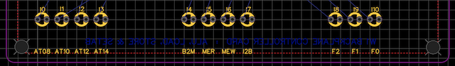
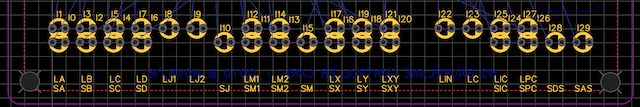
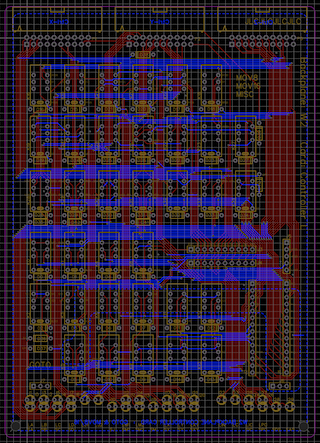
I now need to place the relays, diodes and card interconnects. This often involves just moving things around until there’s a nice fit and the ratlines (showing the connections needed between components) are looking reasonably tidy.
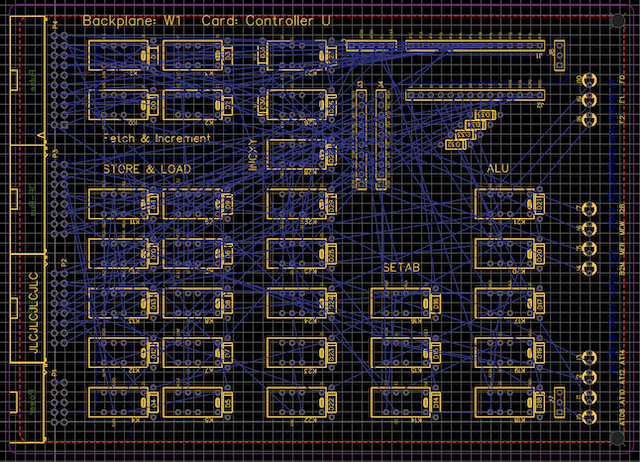
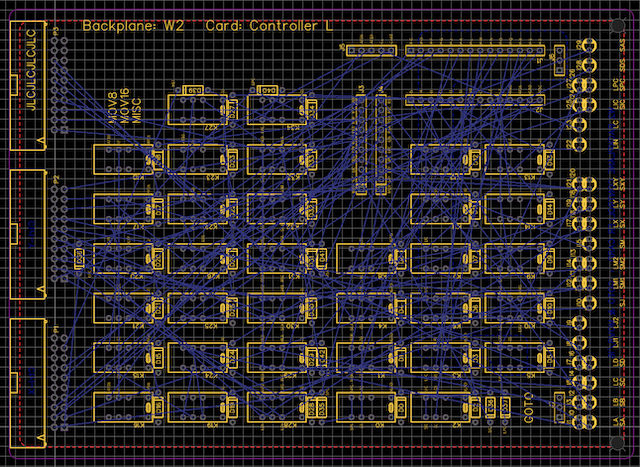
I’ve also labeled the card now I’ve put everything in position. I find this just helps a little when moving on to the most time consuming part of PCB design … laying down the tracks. As with my previous cards I’ll stick with the strategy of laying vertical lines on the front of the card and horizontal lines on the rear. I’m quite tight for room this time as the boards are fairly densly populated with relays so it took a few attempts to get a routing that worked. Here’s what I ended up with:
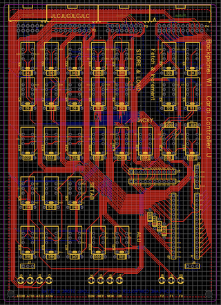
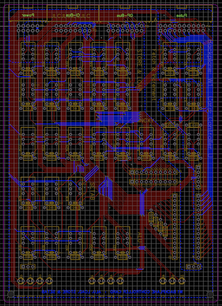
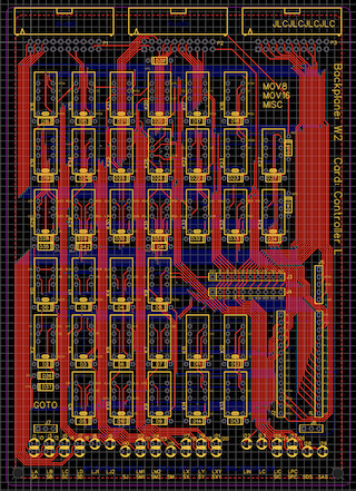
Next I add a copper pour on the front and rear of both cards. As before I have a ground plane on both sides (to ensure ground can get around any areas where there’s a lot of tracks) and then route a ‘power river’ through the rear ground plane.
Finally then I just have a good close up inspection of the board to make sure everything is placed well and tracks are routed properly. There’s several built-in tools that help with this such as the DRC which’ll check that pad sizes, track widths, spaces between items and so on are within the abilities of your chosen manufacturer. In my case I’m well away from those minimum tolerances. Another good idea is to produce a ‘realistic’ image of the final board design to have a last visual check:
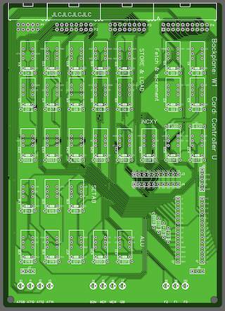
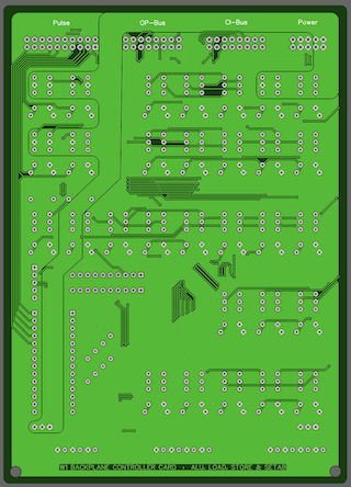
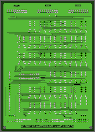
If you’d like to take a closer look at any of these you can find the full colour previews in PDF format here for the upper card and here for the lower card. There’s also another version here for the upper card and here for the lower card which seperates the layers out.
That’s the controller design fully complete and all I need to do now is send it off to the manufacturer and wait for the PCBs to arrive in the post.