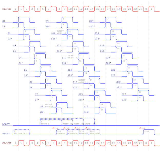
In my last post I extended the 8-cycle FSM (finite state machine) design all the way up to 24-cycles so that we can run longer and more complicated instructions. In this case we’re looking to implement the GOTO instruction so that the computer can perform branching.
As a recap here’s the outputs from the newly designed FSM:
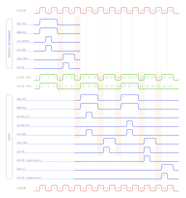
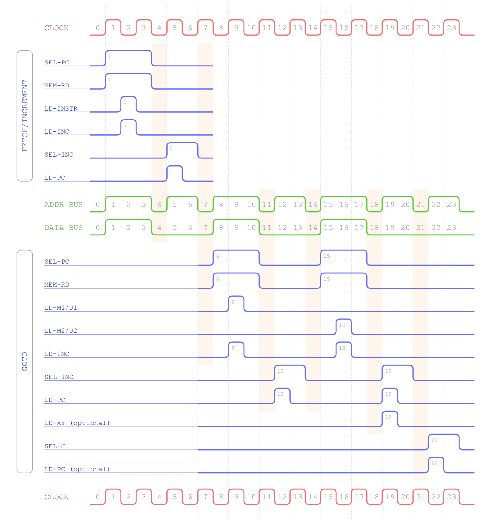
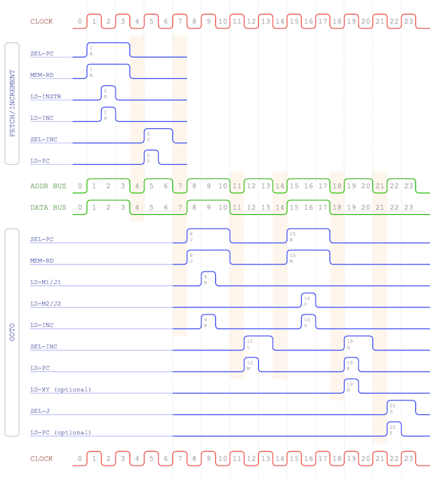
… and here’s the timing chart that we’re trying to obtain:
You might be able to spot that some of the outputs are exactly what we’re looking for … they’re the right pulse for the right duration of time. Some of the pulses we need though can be obtained by combining the outputs together. Jumping straight to it then here’s the pulses that can be derrived from the FSM outputs:
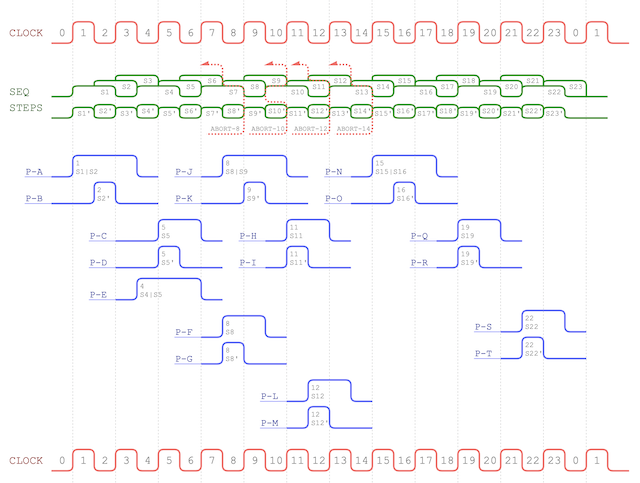
Some of these pulses we already had, of course, in the 8-cycle sequencer … pulses like A, B, C and D which are used in the fetch/increment cycle (shown in the GOTO timing chart above) at the begining of every instruction. For the rest of the GOTO instruction we’ll make use of pulses H - K, N, O and Q - T. If you compare the GOTO timing chart with the pulse chart above hopefully you’ll be able to see the relationship between timing and pulses.
So, we know what pulses we want and how they are derived from the FSM outputs but how is that implemented in the schematic? Well, in the majority of cases we’re just taking a FSM output directly but where we’re combining outputs we can just use diodes as that will give us the ’this OR that’ type logic we need:
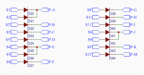
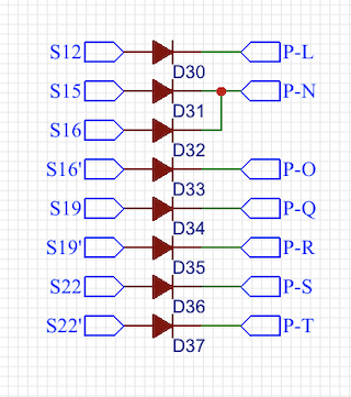
As before with the FSM there’s additional pulses here that we’re not using just yet but rest assured they’ll be needed when we add more instructions to the computer.
So, now we’ve got the required pulses I can update the GOTO timing diagram showing which pulse is used at each point:
It’ll be the controller, of course, that implements the behaviour shown in the timing diagram above (firing the appropriate control lines at the appropriate time) but we have everything we need now to finish the design of the sequencer in the meanwhile. In my next post I’ll cover the final design and PCB layout for the sequencer.