It’s time for the oddly therapeutic part of designing a PCB … laying out the board. In my last post I covered the schematic design and so we now have all the components required for a 16-bit register captured in my design program of choice (EasyEDA) along with how each component is connected to everything else. The next step is to generate a PCB layout from that schematic … and I say ‘generate’ which perhaps makes it sound like it’s a ‘click of a button’ type thing … well, clicking the ‘create PCB’ button results in this:
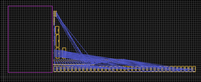
As the schematic doesn’t define any sort of physical location for each component the PCB designer starts off by placing all the components in neat rows by the side of the board. The blue lines you can see are called ‘air wires’ … these are the required connections between components that we’ll have to lay down as tracks on the PCB. The ‘game’ at hand then is to fit all the components on the board and lay down all the required tracks until no air wires are remaining.
Most PCB design tools have an auto-layout feature of some kind and these can be useful to get a feel for how things will fit but ultimately there’s a bit of an art to board layout. You could give the schematic to 10 different engineers and you’d likely come out with 10 different PCB layouts - it can be quite an individual thing. Anyho, here’s a closer look:
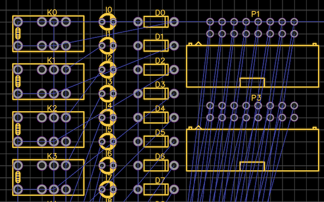
Each of the components that appeared in the schematic has an equivalent ‘footprint’ that defines it’s physical dimensions, outline and the shape/position of the holes. You can find footprints available in online libraries for most common components but if needed you can create your own or tweak an existing one. In the case of the relays here I’ve used a generic footprint for that size & leg pitch and then changed it as needed. One of the key things to check is the size of the pads, hole sizes and solder mask reveal:
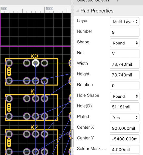
Note the unit of measurement here is ‘mil’ which is a thousandth of an inch. You can change this if preferred but most manufacturers will list their manufacturing tolerances/abilities in mil. In particular you need to keep an eye out for smallest hole size, track size, distance between tracks etc. Keeping to a limited selection of hole sizes can also reduce the cost of the board manufacturing being as it saves tool changes and so on. In this case the holes for the relay legs are 51.181mil which is 1.3mm. As it happens this is way bigger than I needed (the matrix board I’ve been using so far have 1mm holes). The pad size is 78.74mil (2mm) and then there’s a 4mil (0.1mm) clearance around the pad before the solder mask covers the copper. It’s worth spending some time on getting all the pads right before moving on.
The next job is set up the grid and physical board outline:
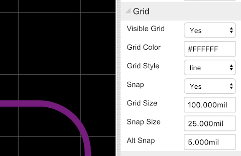
Here I’ve set the grid size to 100mil which is 0.1inch as this matches the hole pitch on the matrix/pad prototyping boards I’ve been using so far and this’ll make it much easier to place the connectors and LEDs to match the other cards. I’ve set the snap size to 25mil so that when placing tracks it’ll snap to 1/4, 1/2 or 3/4 of the distance between grid points meaning I can, in theory, fit 3 tracks between pads easily (and making this process as easy as possible is crucial as there’s a lot of tracks to route around components).
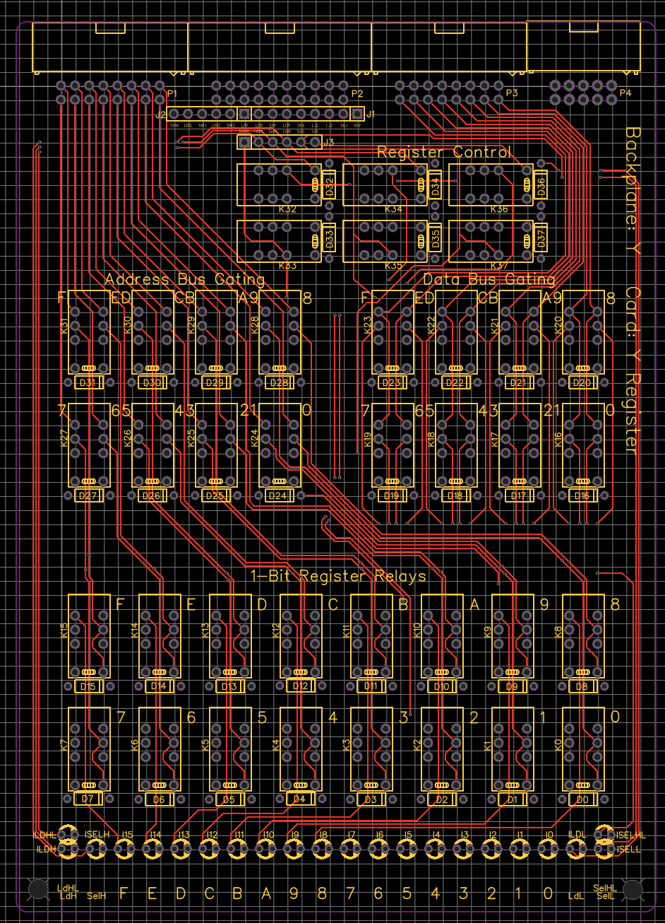
For the board outline it’s simply a case of drawing the lines in the right place and at the required length. As I’m keeping the size the same as the existing matrix/pad boards then that’s 160mm by 115mm. For the same reason I’m rounding-off each corner by drawing arcs. Note that the board outline is positioned so that the grid lines up with where the holes are on the matrix/pad boards so, again, components can be placed accurately to fit the computer backplanes. When the board is manufactured it’ll be milled out along this board outline so you can, if wanted, make your board any shape you like.
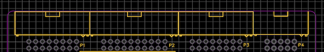
With the board outline sorted and grid positioned/sized we can start laying out some of the components. It’s usually best to start with the components that depend on being in a particular place on the board. In our case that’s the LEDs at the front and the connectors at the back.
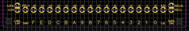
I’ve also added some of the silk-screen legend too at this point which will appear in white text on the final product. This step is often left until the end of the card design process but being as these LEDs aren’t going anywhere it makes sense to get this bit out of the way (and it’ll help me identify what’s what when I start laying down tracks). You can also see the two non-plated drill holes at the front of the card to match the matrix/pad boards.
It’s worth printing the design out at this point at 1:1 scale and comparing it to the components and to other cards to make sure the dimensions are coming out well. The more checking you can do before laying down tracks then the more time and frustration you can save. That’s not to say that re-work is totally avoidable and sometime’s you’ll get a PCB layout nearly completed only to realise something is missing that forces everything to be moved around.
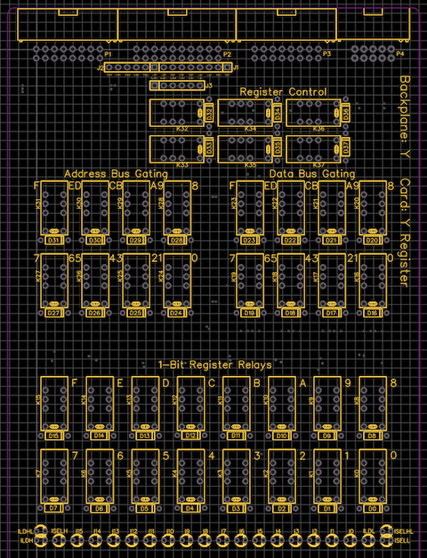
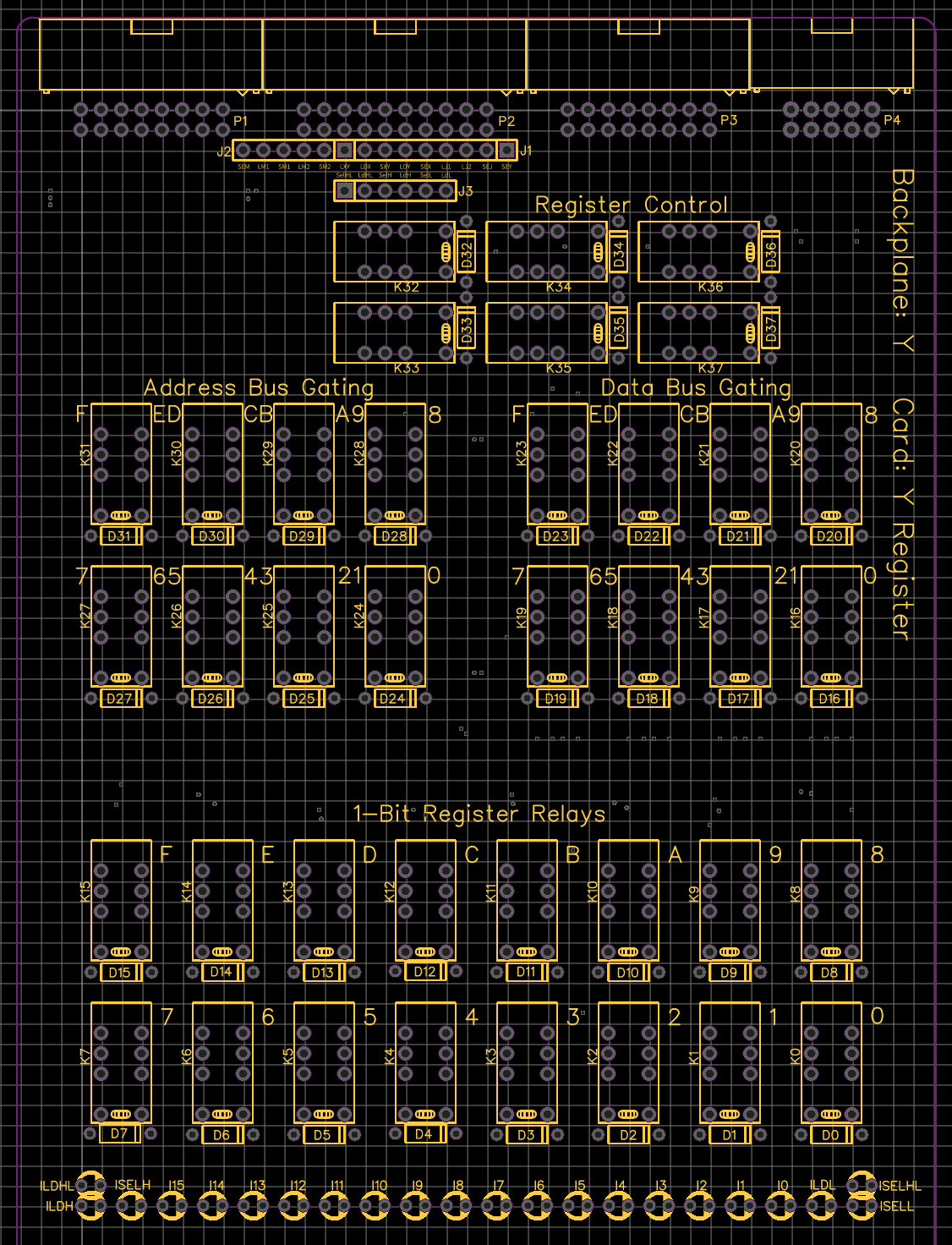
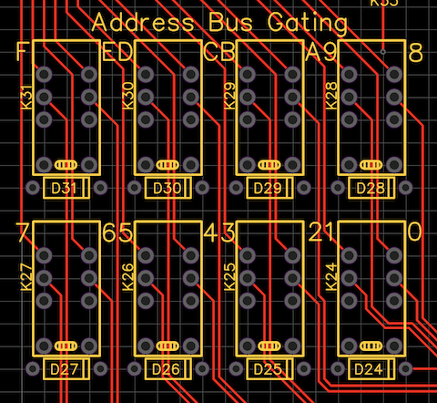
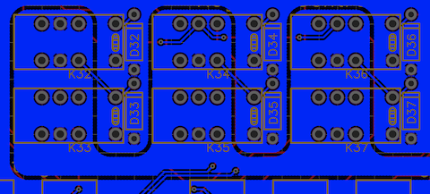
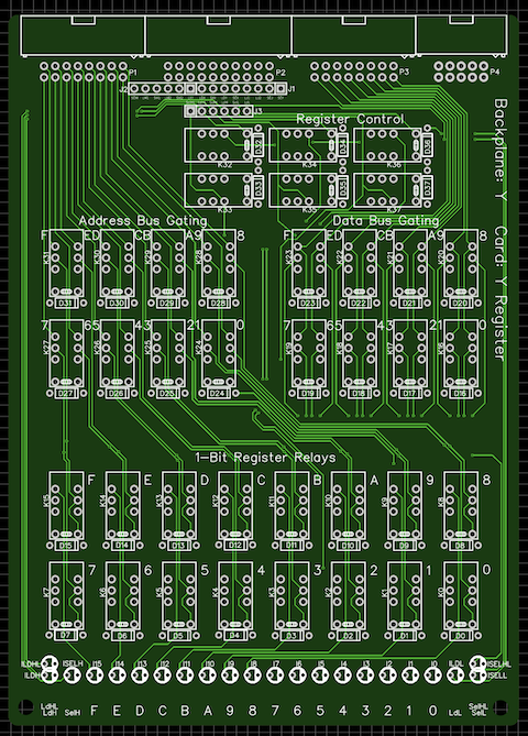
With other components placed on the board we can now move on to placing the relay units (relay plus diode). Having a good understanding of the schematic and where the ‘functional blocks’ are can help with this step. Failing that it’s a case of trial and error moving things around to you get something that’s pleasing to the eye and looks like there’s a good chance of laying down the required tracks.
Again, I’ve got ahead of myself and added some of the silk-screen legend just to help keep track of what’s what. With the components now laid out we can have a go at laying down some tracks:
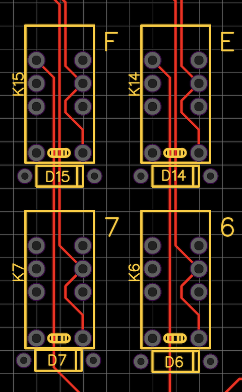
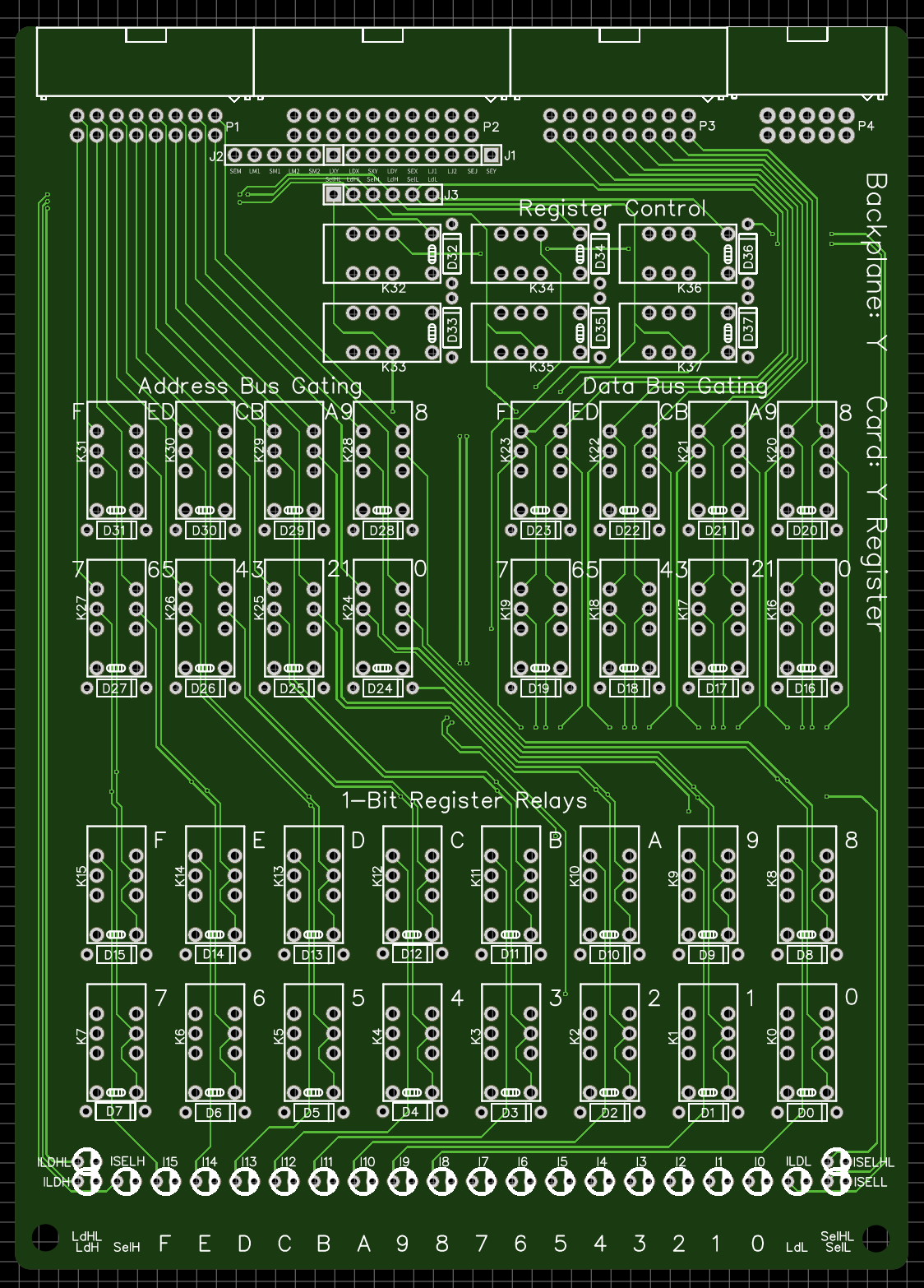
Here the red lines are tracks laid down on the top of the board which is where the majority of my signal tracks will be placed. As each track is laid down the blue air wire will disappear and we’re one step nearer to a completed design. A good general track design strategy to try and place signals on one side of the board vertically and horizontally on the other. Here I can generally go vertically on the top as most signals are passing from the front of the card to the rear.
We can keep going in the same way laying down as many tracks as possible. Eventually, if there’s enough air wires hanging around, you’ll need to have tracks cross over each other. This is where we’ll need to drop a signal to the other side of the board using a ‘via’.
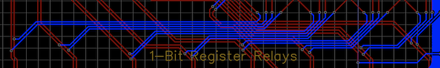
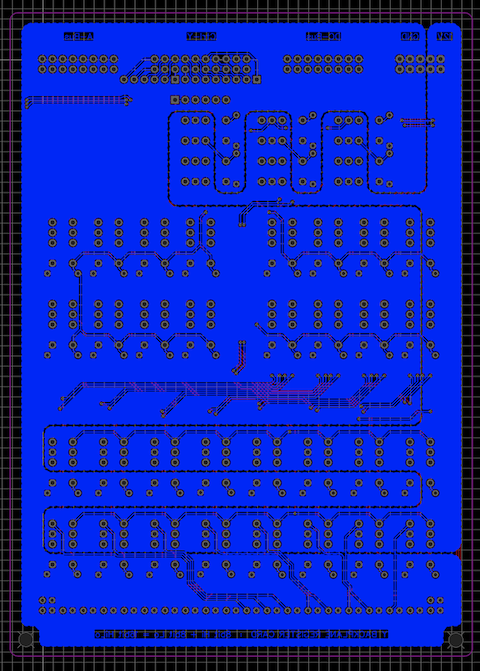
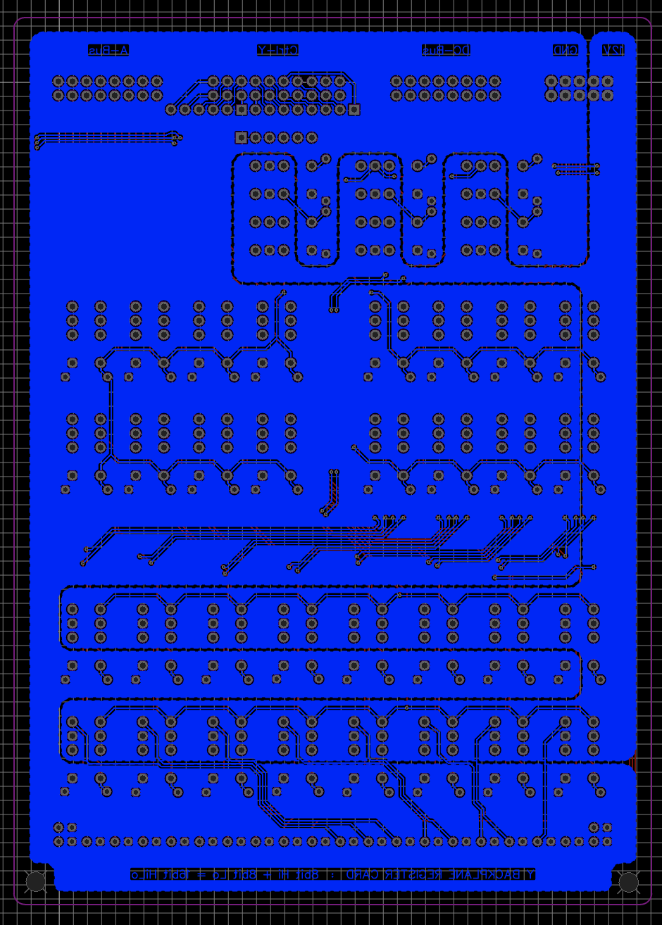
A via is a tiny solder filled hole that goes through the board and connects a track on one side of the board to the other. Here the blue lines are on the bottom of the board and used to get the tracks coming down the right half over to the left half where they’re needed further down the board. Again, these bottom tracks are kept reasonably horizontal. At this point we have our upper and lower signal tracks all routed. Here’s all the upper tracks:
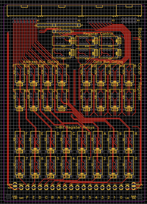
With all signal tracks routed we’ve now got to turn our attention to the power and ground lines. Each relay needs its coil grounding and a lot of them take power to some of their contacts to be able to create the outgoing signal lines. A typical solution to routing these power and ground lines is to create copper planes. In a four layer board you’d have signals on top and bottom and then a whole ground plane and a whole power plane. In my case I’m making a cheaper two layer board and so I need to fit the planes within the two layers I’ve got. To create a plane you draw a shape for the ‘copper pour’ and name it the same as the power lines:
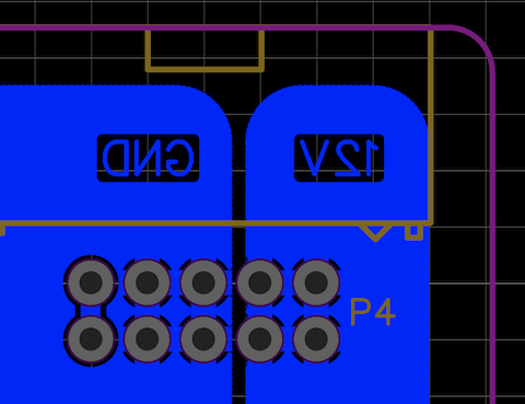
Note the connections between the planes and the power connector pads … these appear as ‘crosses’ and this is for thermal relief. Without these soldering would be a nightmare as the heat of the iron would be wicked away by what is, in effect, a giant heat sink. These thermal relief lines limit the amount of heat wicking making soldering possible. In this case I’ve decided to place both planes on the bottom of the card as I was pretty sure I could make it fit.
I’m quite lucky on my PCB as I’m not doing anything high frequency or AC based and so I have less to think about. If you are doing something like that then you have to be quite careful with your planes. Large ground planes are quite nice for sinking stray RF but also placing one place above another can actually create a capacitor (albeit with quite low capacitance). In general you also need to work out how much copper area is between components and how much current they draw.
Here you can see the ground plane coming in from the top and the power plane coming in from the right. As I’ve got signal tracks running through this area too I have to be careful to make sure I’m not cutting off any power/ground connections or making the copper too thin/narrow. Again, each pad connection to a plane has thermal relief on it. Here’s the completed planes for power and grounding:
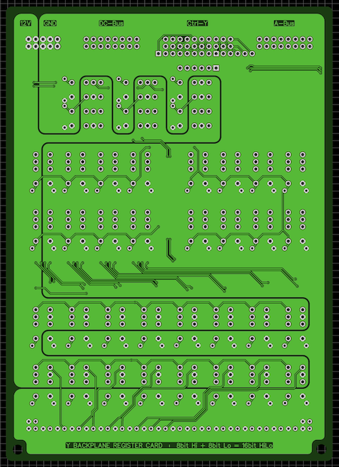
… and with that we’re pretty much there. All that’s needed now is a close check of absolutely everything … check, check and check again. Although minor mistakes or errors can be patched up after the card has been manufactured it’s not ideal and anything major will need another trip to the factory. Fortunately EasyEDA offers some nice tools for inspecting the design (as do other tools) … the first one is the ‘photo view’ which allows you to display the finished card in your chosen mask colour:
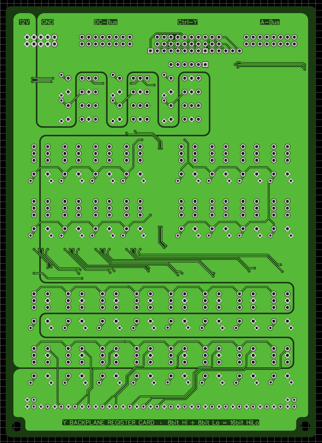
… and if that’s not enough you can even view your card in the 3D viewer …
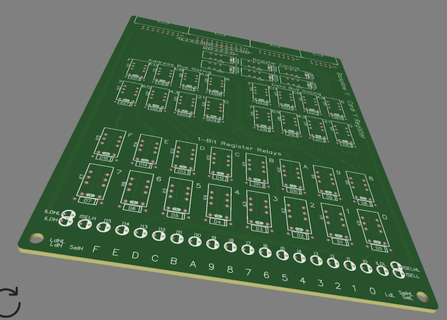
Once you’re happy with your design (and you’ve given it a thorough check) then you can push it to your chosen manufacturer. In my case it’s JLCPCB who have a five board minimum order but given how cheap they are it’s not a problem.
So, once the cards have arrived it’s on to soldering and I’ll cover that in my next post (along with a YouTube video). If you’d like to take an even closer look at the PCB design for this card you can find my original design files on EasyEDA here. There’s also a design for another PCB there which will be used as a mounting plate for the LEDs along the front of the card to keep everything nice and neat.