In my last couple of posts I’ve been building up to a change of approach in how I’m making the cards in my computer. This is mainly because I can’t face the monotony of hand building the upcoming register cards (which I’ll need three of so it’s triple the procrastination holding me back). The obvious solution to all of this is to create a Printed Circuit Board (PCB) which will cut out most of the trickier soldering and pretty much all the repetitive wirewrap … and that looked like the way to go until I had a go at hand crafting a simplified PCB for the Y backplane and I realised it’s not as easy as it might otherwise appear.
Well OK, yes, the Y backplane did work but not without a lot of tweaks and repairs and that was just a simple single sided PCB. The registers boards are far more complicated and there’s no way I can design a single sided board without having lots of lines crossing over each other. The ‘fix’ here is to make a double sided PCB with tracks on both sides and with vias (tiny solder filled holes) passing the signals/line from front to back etc. I did a few rough drafts on paper to get a feel for how the board would look and what lines would need to go where but it soon dawned on me that I’d end up with more work than my original approach and with likely more mistakes and problems.
So, what to do then? Well it seems that maybe it’s time to wave my little white flag, accept some level of defeat and hand the hard work over to the ‘big boys’. That’s right, I’ll farm out the manufacturing of the PCB to a professional outfit who can do a decent job. In some ways this feels a little bit like ‘cheating’ although it wouldn’t be the first time I’ve taken a shortcut (using a modern memory chip rather than a house full of relays for example). I’ve kind of convinced myself that getting someone else to make my PCBs is acceptable though as I’m not setting out to prove I can make a computer from the most basic of ingredients just to make a computer that works, has some connection with the original relay computers and ultimately is enjoyable to build (this is a hobby project after all).
There’s quite a bit of choice when it comes to picking a PCB manufacturing house but after several recommendations I’ve gone with JLCPCB. Although there’s a minimum order quantity of 5 (which works out quite well for my register cards) the per-board card is impressively cheap but even more impressive is that they have a free design software offering EasyEDA which makes it easy to design your PCBs. Yea, I guess there’s a bit of vendor lock-in here perhaps but it looks like you can export to other file formats and there’s a native Mac client which pretty much had me sold.
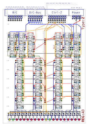
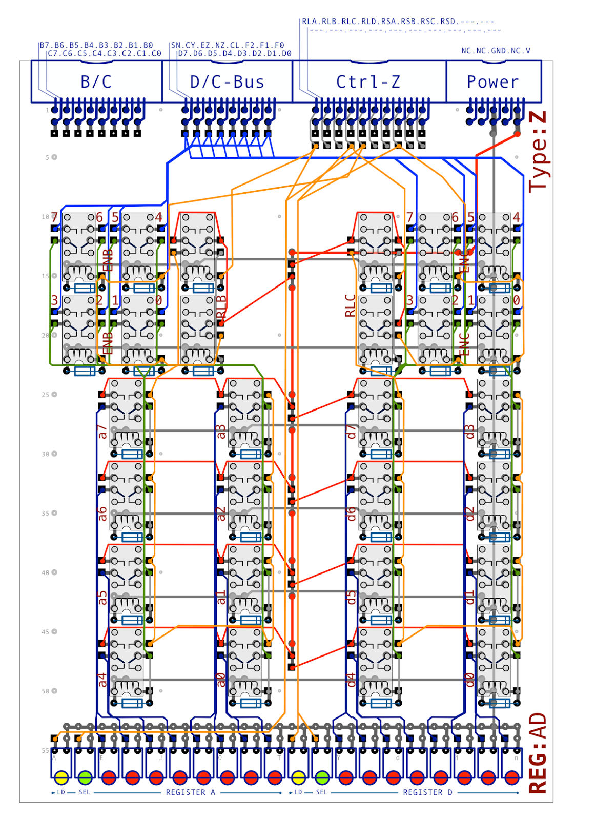
So, a fair bit of preamble there then but that gets me to the point where I’m now ready to design a register card in EasyEDA. My goal is to design a card that has two 8-bit registers that read and write from/to the data bus (much like the registers built so far) but that can also be paired up in to a 16-bit register that gates to/from the address bus. Looking back to the design of the 8-bit A/D register we ended up with this:
This schematic was produced in OmniGraffle on my Mac and is, to all intents and purposes, just a picture. What makes EasyEDA such a leap forward is that doing the schematic design in that captures what the components actually are and how they connect to each other. This makes it easy to produce lists of parts and ultimately to transform the schematic into a PCB. Anyho, I’m getting ahead of myself. I need to reproduce the OmniGraffle design in EasyEDA … let’s start with the most basic element … a 1-bit register unit:
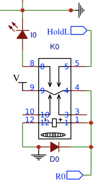
R0 in the schematic is the input/output to the unit. Supplying power to this line activates the relay and then as long as power is supplied to the Hold line that relay will be kept activated. Dropping the Hold line resets the relay. All the basic functionality is handled on the right hand side of the relay. The left hand side allows a LED to display the current state of the register bit without complicating the primary circuitry on the right. As always there’s a flyback diode over the relay coil to absorb the spike when the relay is deactivated.
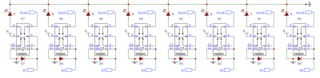
From this basic 1-bit register design it’s fairly trivial to connect eight units together to make an 8-bit register:
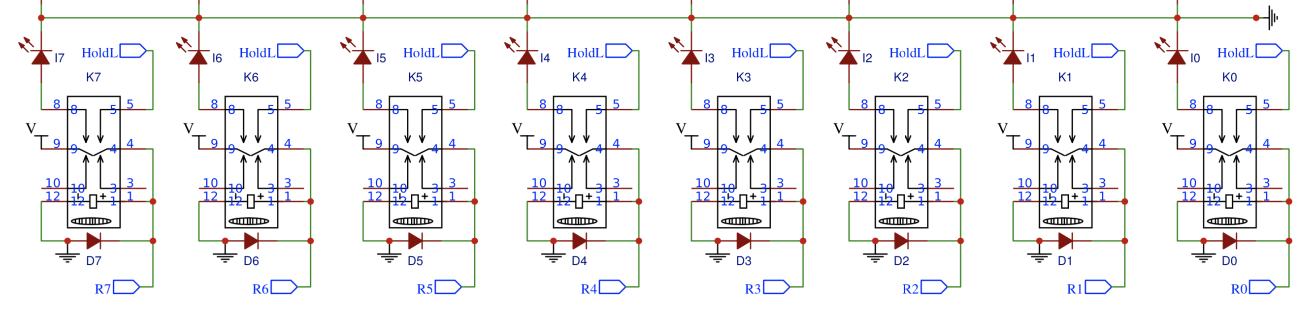
Note that the Hold line is shared across all the relay ‘bits’ so that the register can be held/cleared as one but that each individual ‘bit’ has its own input/output line R0-R7. To get two 8-bit registers we just double up the design:
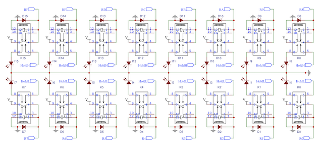
The data input/output lines continue on from R8 thru RF but note that the hold line is different. The first 8-bits use a HoldL line and the next 8-bits use a HoldH line. This refers to High and Low hold lines which allows either the high (R8-RF) or low (R0-R7) register to be held or cleared as required. Effectively each 8-bit register can be loaded/cleared independently as and where required. We’ll come back to the control circuitry that drives this in a bit but let’s look at the bus gating next:
In this case we’re looking at the gating for register bits R6 and R7 (the highest bits of the low 8-bit register). R6 and R7 connect to the register bits in the schematics above and the gating relays allow that input/output line to be gated to either D6 and D7 of the data bus or A6 and A7 of the address bus. EnL enables the gating to the data bus and the line at the bottom of this schematic (EnHL) gates to the address bus. Again, we can extend this design out to gate a full 8-bit register:
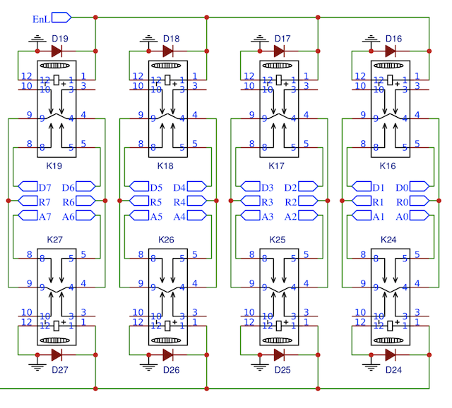
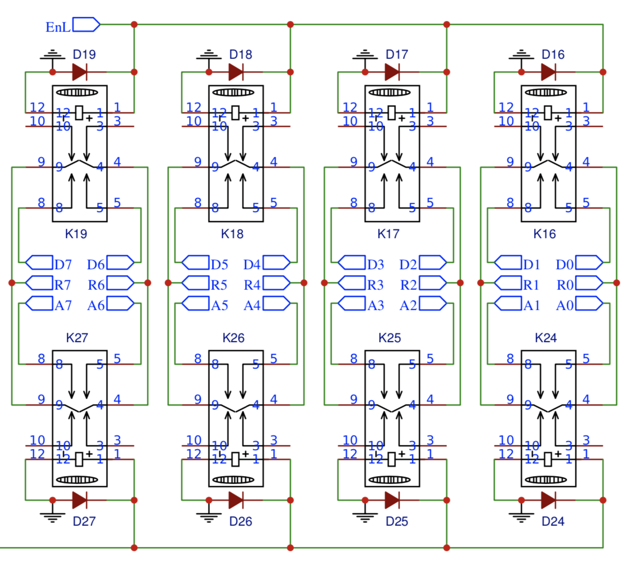
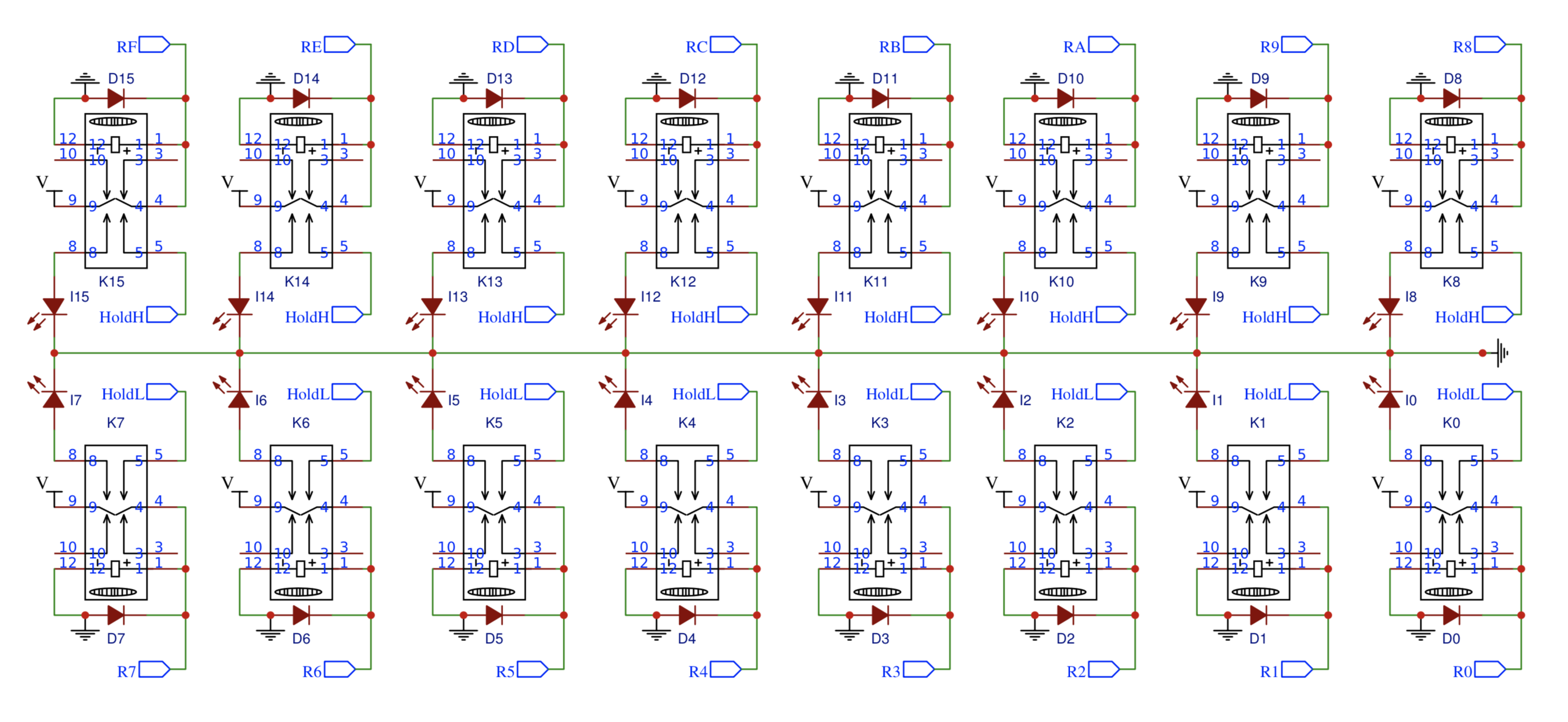
… and onwards to gate the two 8-bit registers as independant units or together as a single 16-bit register …
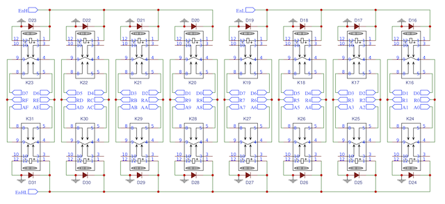
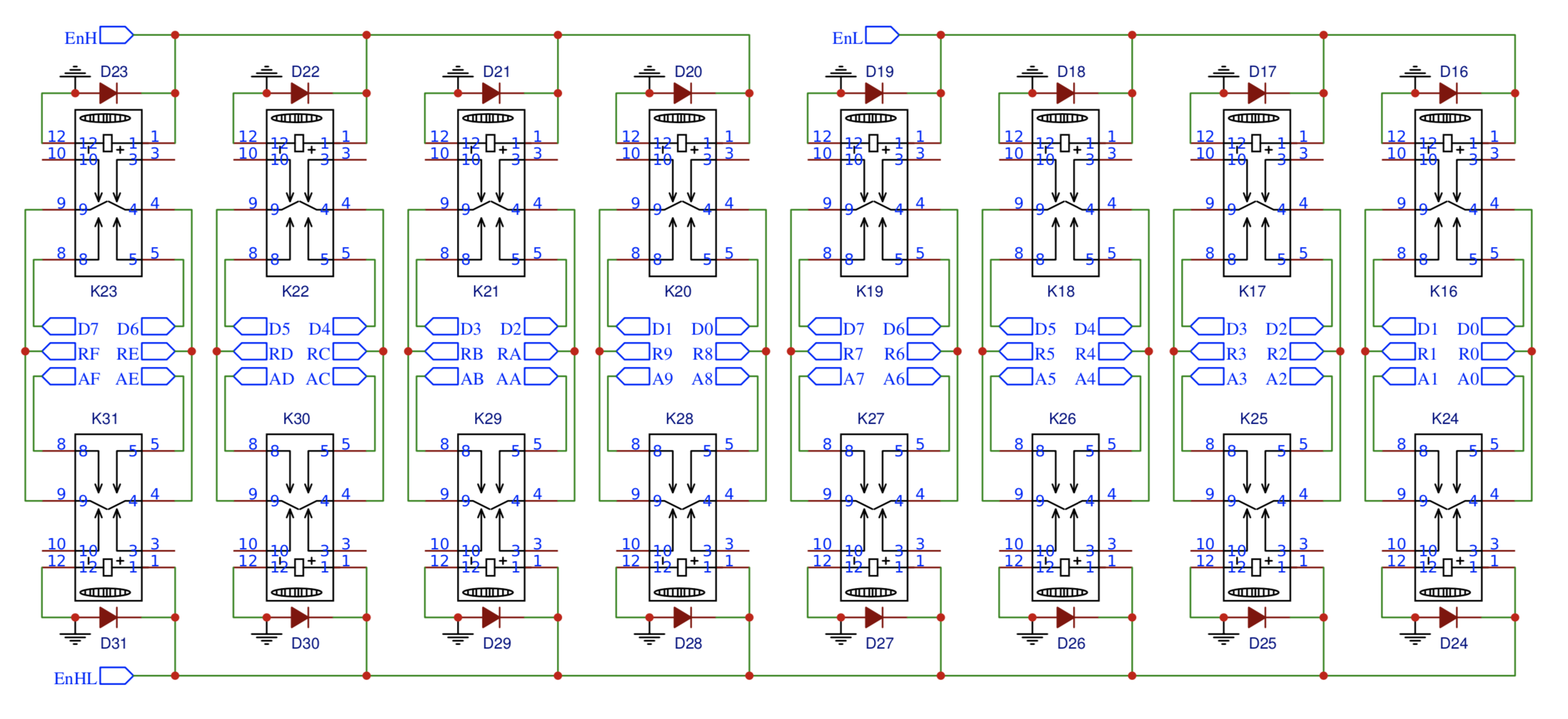
Note that EnL (lower 8-bit register) gates R0 - R7 to D0 - D7, as you’d expect, but EnH (upper 8-bit register) gates R8 - RF also to D0 - D7. This makes sense because there’s only one 8-bit data bus and if you wanted to load the full 16-bit register from there you’d need to load the lower 8-bits first and then the upper 8-bits. Of course, there only needs to be one EnHL for the 16-bit address bus which gates A0-AF to R0-RF. Right, that’s the register relays and the gating … let’s return to the control circuitry:
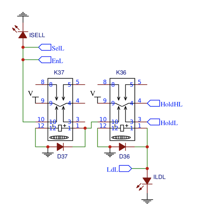
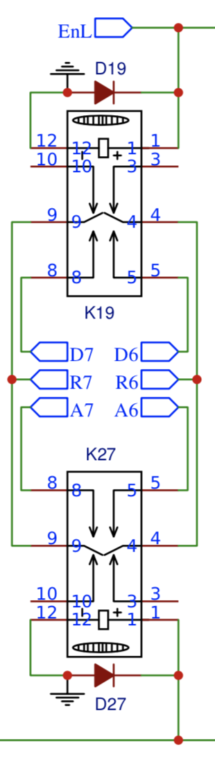
This handles the HoldL and EnL lines we’ve already seen for the lower 8-bit register. The inputs to this circuit are SelL to write to the data bus and LdL to load from the data bus. Selecting the register to write to the data bus is very easy … we just activate the gating relays. Load is a bit more involved however. To load we need to disconnect the hold line (which clears any value held in the lower register) but also we need to activate the gating relays to bring in the value on the data bus. Interestingly here the HoldL comes in from HoldHL and this is so that by default both 8-bit registers are holding their value and if we want to load one independently we need to veto that hold. If both registers are being loaded together then the HoldHL line is dropped which achieves the same as far as holding is concerned. We can now repeat this design as you’d expect:
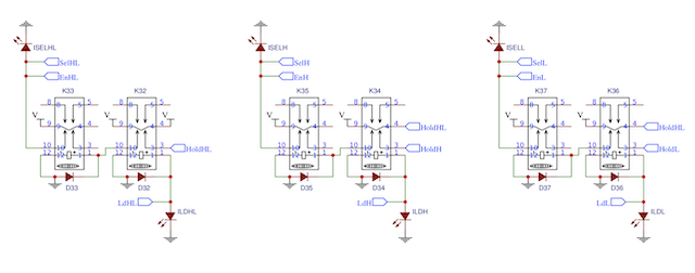
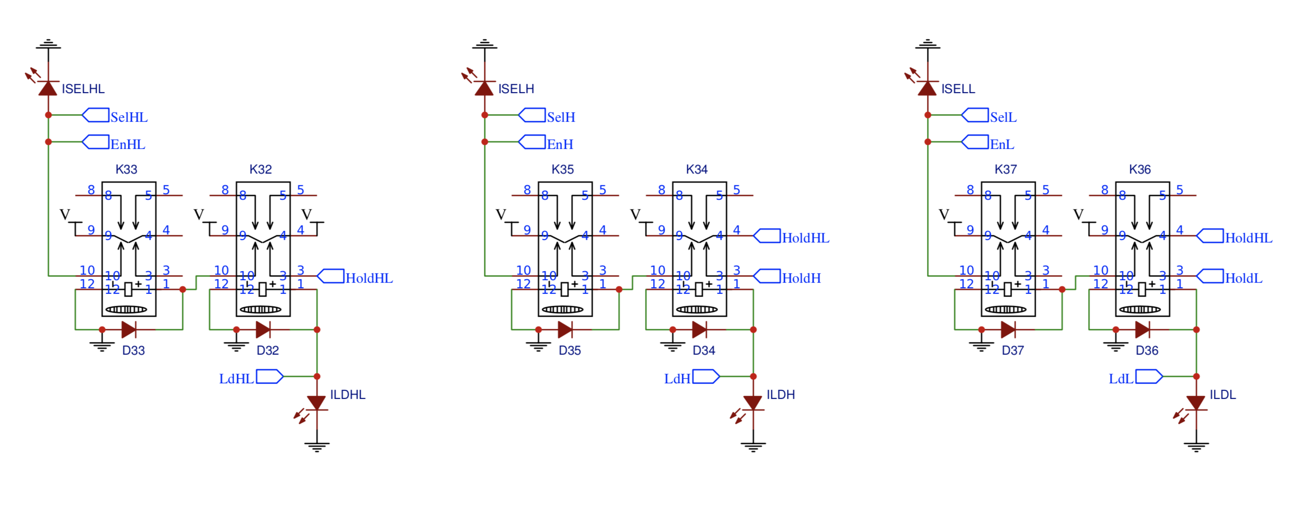
So that gives us the three main components of a register: storage bits, gating and control. We finally need a way to connect the register to the outside World and that’s where the card connectors come in. In the schematic they’re represented as follows:
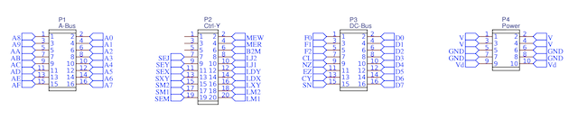
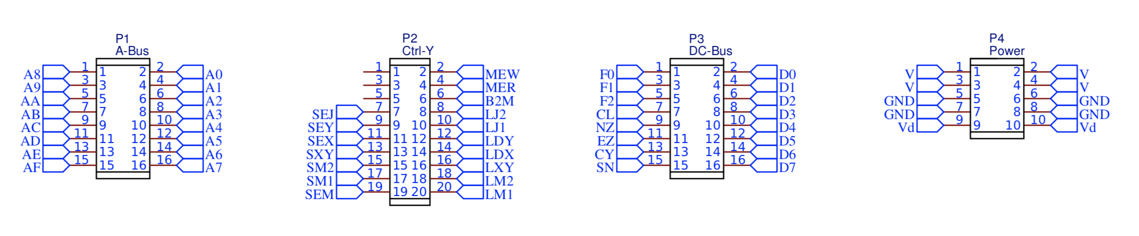
This now brings us to one final minor problem. I want to make three 16-bit register cards however there’s something stopping them from being created identically. The three registers will be M (M1 and M2), J (J1 and J2) and XY (X and Y). The difference here is that each will respond to different control signals to ensure that if you’re loading, say, the lower 8-bit M1 register you don’t impact to lower 8-bit X register. I need some way of ‘configuring’ each register card to make it M, J or XY specific. The simplest solution here is to have a jumper block that I can set a wirewrap link on:
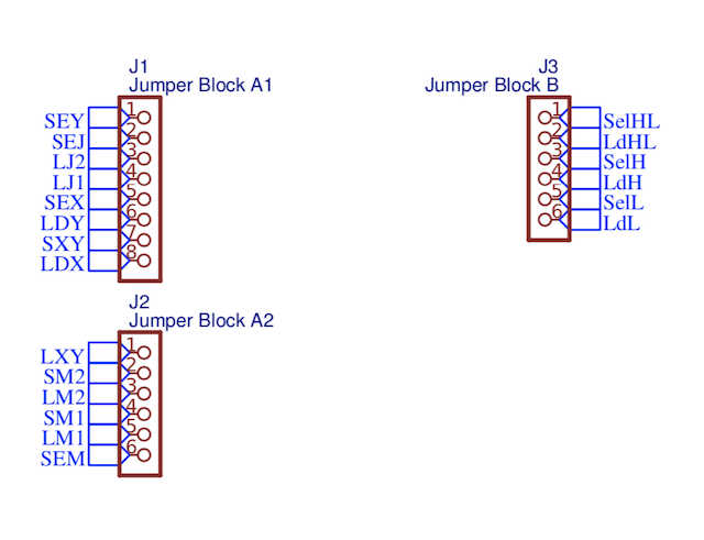
… and with that we have a complete design for a 16-bit register with independently controllable upper and lower 8-bit ‘sub-registers’. As usual there’s a version of the full design here in PDF format. In my next post I’ll go through how this schematic becomes a PCB design that can be sent off to JLCPCB for manufacturing.