In my last post I touched on how the repetitive nature of making register cards has been putting me off progressing my relay computer. If you’ve followed my blog (over the years) you’ll have witnessed the construction of the general purpose registers A, B, C and D along with the specialised registers in the incrementer and program counter. Each register card follows the same construction pattern: solder down LEDs, solder down relay sockets, solder down wire wrap posts, solder ground and power lines, wire wrap, wire wrap, wire wrap, wire wrap, etc, etc, insert relays in sockets. Tedious, tedious, tedious.
I’m being slightly insincere there of course … there’s far worse things in the World than having to construct a register card (first-World problem etc) but this is supposed to be an enjoyable hobby … and I’ve got an incredibly short attention span. What’s needed then is a change of approach that will streamline the construction process and have me learning new skills to keep me entertained and engaged.
Looking at the current construction process in my first paragraph above you can see most of the time is spent soldering sockets and wire wrap posts with the wire wrap itself taking a close second place. So, what could be simplified here? One option is to solder the relays directly to the board. This cuts out the turned pin sockets (which are quite expensive) but means replacing relays is a lot harder. Given I’ve had no relays fail so far I think this is an easy saving. What else?
The cards currently use wire wraps to connect all the various relays, LEDs and backplane connectors together. I chose this technique originally as it’s easy to fix mistakes or make modifications. As time’s gone on I’ve found, apart from the occasional mistake, I’ve not really called on this flexibility so I could go for something a bit more permanent.
Hopefully by now any of the electrically minded out there are screaming out ‘why don’t you make a printed circuit board (PCB)’. Well, yea, I hear ya. Now, of course, I’ve always been aware that PCBs exist and can be made at home but I originally felt the mess-free, mistake forgiving, wire-wrap technique would suit me better. That opinion is now about to change. My thinking now is that I should be able to make a PCB relatively quickly … although I suspect the hole drilling is going to be the new boring thing (no pun intended) … and if I do make a mistake then I can still use the kynar wire to modify the board layout.
Right, that’s been a lot of text … let’s have a picture …
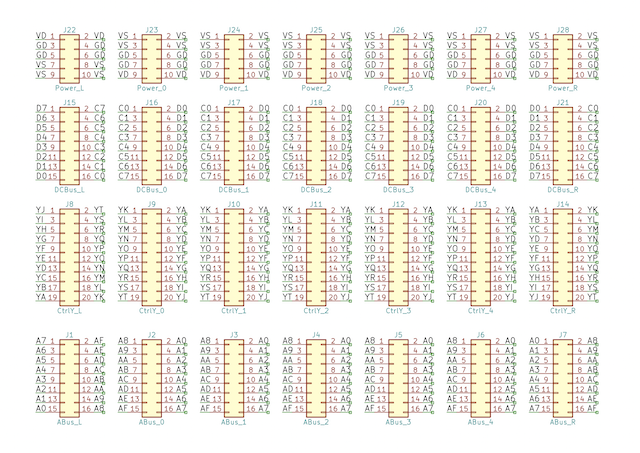
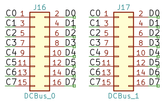
What?! OK, so I should probably have warmed you up for that. One of the other problems I created for myself a long time ago was designing all the schematics by hand using OmniGraffle on the Mac. Obviously I used the magic of copy/paste to make things a bit easier but still, I’ve spent a lot of time drafting the schematics so far. If I’m going to get slightly more ‘grown up’ and make PCBs then I should probably use more appropriate software … and my software of choice this time has been KiCad. This open source cross platform package is specifically designed for the production of schematics and PCB layouts and it’s the schematic for the Y backplane that you’re seeing above. Here’s a close up:
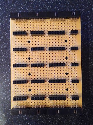
Backplane Y seemed a good place to start off my PCB experimentation phase as it’s relatively simple … just connect all the sockets together. Previously I’ve made the other backplanes by ‘daisy chaining’ a ribbon cable over the back of stackable header sockets and whilst this has sufficed I have had some flaky connections on the Z backplane. Here’s what the Z backplane looks like:
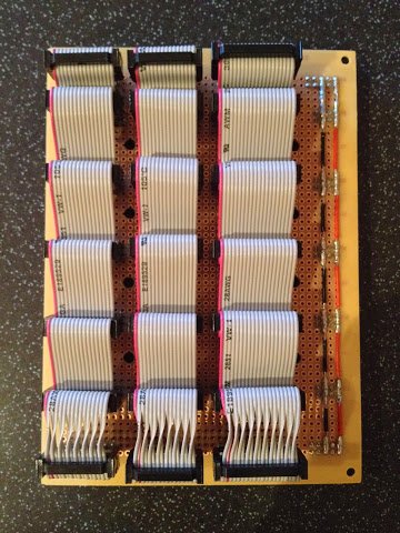
Given that a PCB version of the above does away with the ‘daisy-chain’ we should get a much more robust/simpler card that’s, in theory, easier to construct. Looking back to the schematic above (for the Y backplane) you can see there are four busses that run horizontally across the schematic. Top down these are the power bus, data/control bus, control Y bus and finally the address bus. Going vertically left to right you first have the incoming busses to the backplane followed by five columns for each of the five cards and then the outgoing busses at the end. If you look at the picture of the Z backplane above you’ll hopefully see the similarities.
Each connector in the schematic has each individual pin labeled and this tells KiCad that all pins with the same label are meant to be wired together. The wires themselves are not drawn in the schematic as it’d make it far too busy/confusing to look at. One thing that maybe needs a special mention is the connectors at the far right and far left. These are right angle IDC connectors that because of the way I orient them when soldering down they end up with odd pin numbers. When the schematic is transferred to the PCB designer it all works out. Speaking of which:
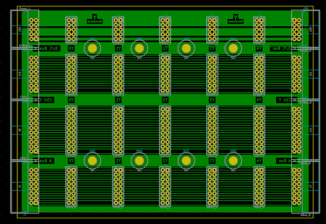
There’s a bit of an art to laying out a PCB and when you first open the PCB editor you’ll find a massive jumble of component pads and connection lines. I personally quite enjoyed moving all the bits around and laying down the tracks but your own milage might vary. You may have noticed the image above is mirrored and that’s because you design the board from the front. In this case all my copper tracks are on the back of the board but you might also have tracks on the front too (a double sided board). Incidentally, that’s the other reason I’m starting with the backplane as all the copper is on one side … making a double sided board is far more challenging but will likely be required for the register cards.
Here’s a close up on the PCB …
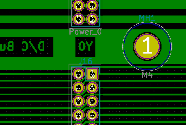
Once you have a PCB designed to your liking there’s a couple of routes onwards. You can either farm out the construction to a PCB house or make it yourself. Needless to say the best quality PCB is going to be professionally made but I’ve found that ordering one board can cost not far off the price for five or ten boards … economies of scale. Every board I need however is unique (often similar but still unique) so DIY PCB is the way for me. Again, using KiCad I can output each of the PCB layers giving me a copper track layer, silk-screen/legend layer, solder mask layer and even drilling layers.
I’ve uploaded the schematics and PCB layers in PDF format so you can have a closer look if you like but I’ll leave this post there for now. Next time I’ll have a go at actually making this PCB and so that you can witness the disaster/success unfold I’ll record a video covering the whole process.