In my last three posts I covered the design of the auxiliary control unit which will ease entering and inspecting programs in the computer’s memory. With the design ‘in the bag’ it’s time to get constructing although this time we’re not starting with a blank card …
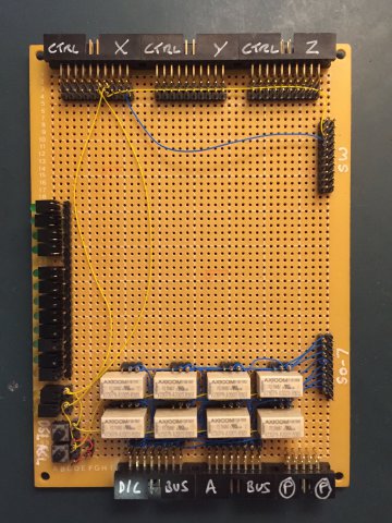
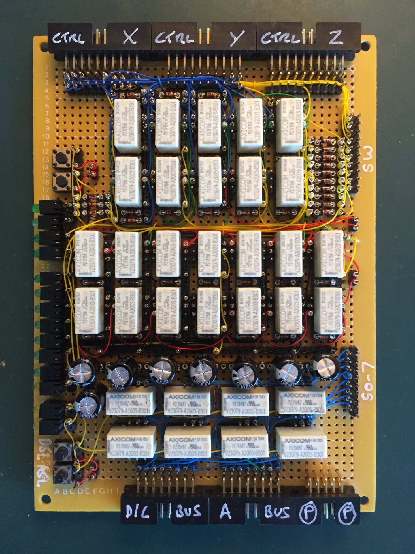
Currently the auxiliary card has the gating relays along the bottom which connect the primary switches to either the address or data bus as required. So far these gating relays have been operated manually but that’s about to change as I add the remaining auxiliary control circuitry which will operate the gating directly. Also on the card are the row of LEDs on the left, card connectors at the top and finally the primary switch connectors on the right. Again, all of these bits will be hooked up shortly as I add the control circuitry. First though let’s get the auxiliary clock built and here’s a reminder of the clock circuit:
… which builds out as follows …
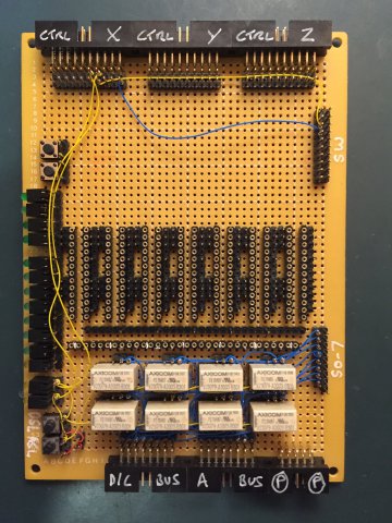
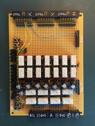
If you’ve got a keen eye you might have noticed there’s eight columns of relays in the diagram but only seven in the picture above. Well, if you look closely at ACL6 in the diagram you’ll see you can actually implement that stage in one relay rather than two and that’s exactly what I’ve done. In the column nearest to the LEDs is a single relay for ACL6 and then another for ACLR.
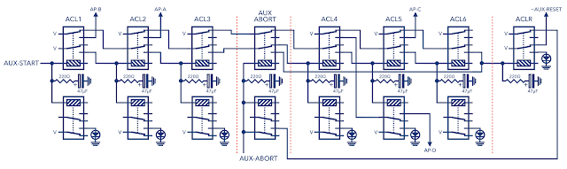
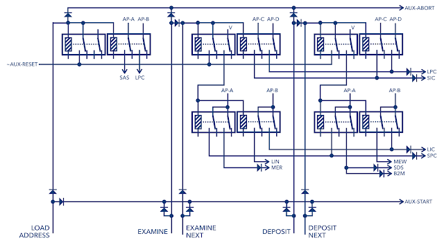
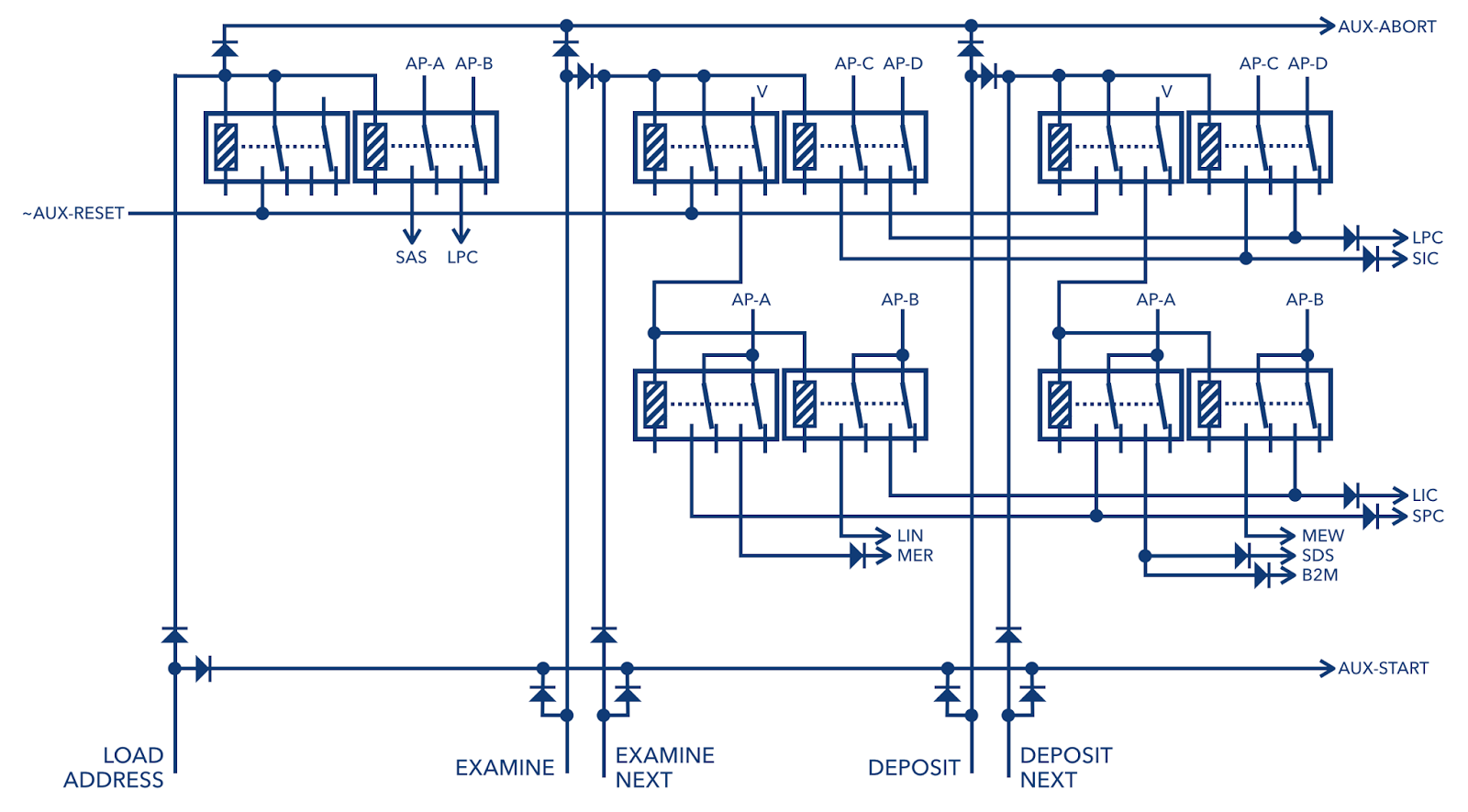
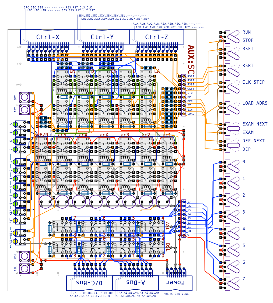
With the auxiliary clock in place the next job is to add the auxiliary control relays. Here’s the schematic we’re looking to implement …
… which builds out as follows …


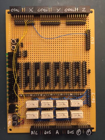
If you fancy a challenge have a go at a ‘spot the difference’ between the two photos above of the rear side of the auxiliary card. An interesting one is the appearance of two resistors soldered on to the backs of two relays (one resistor across each relay coil). What’s going on there then? Well, it’s the afore mentioned ACL6 and ACLR again. The capacitors below the relays form a RC network with each relay coil and that sets how long each relay coil stays energised for. The timing is set for two coils in parallel but in this case for ACL6 there’s only one relay so I’ve added a resistor to ‘make up’ for the missing relay coil (same applies to ACLR). This is one of those things I discovered late when testing the card and so it ‘magically’ appears sometime between the two photos.
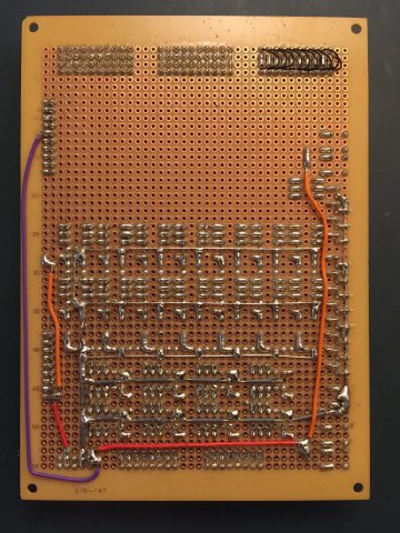
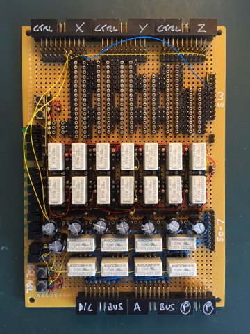
That’s the construction completed so let’s compare the finished card with the design schematic …
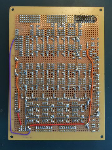
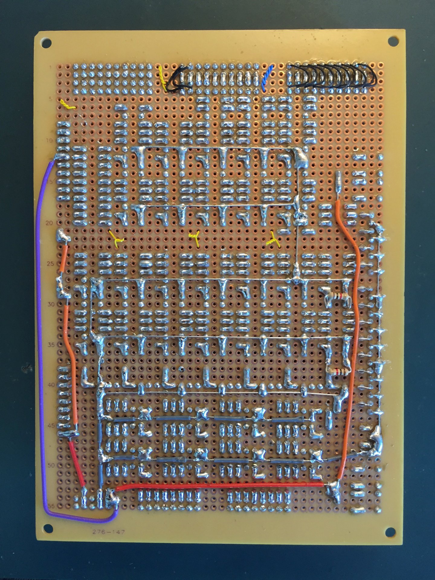
… and here’s the same compared with the rear side of the card …
So the question is now … ‘does it work?’ … well ‘kinda’ but I’ll let the video take over at this point …
This post seems to be doing a lot to test your powers of observation (and perhaps testing your patience too no doubt) … you may have noticed that the photos above don’t quite match the finished article (pause your eyes if you want to guess at the differences). Firstly there’s resistors added over every capacitor to limit the inrush currents and save me from destroying diodes (took me a while before I realised unfortunately … luckily diodes are cheap). The clock schematic at the top of this post does include these resistors and that’s because that diagram was also created post mass diode-ocide. Next difference is the capacitors in the video are smaller than those in the picture (no, they’re not just further away) … the larger ones had a higher capacitance and therefore held the relays on longer which helped when testing the clock circuitry. With that tested I could then drop in smaller capacitors which shortened the clock time and makes each auxiliary operation quicker. So why didn’t I take an updated picture … well, if you’ve watched the video you’ll know the answer to that … queue the music ;)
So, what’s next. Well that pretty much ends this milestone … I now have a computer that can run through a basic program loaded in to it’s memory. It makes sense at this point to checkpoint and reflect on the progress so far so I’ll upload a video covering the instruction set and do another overview video and then I think it’s time to start thinking about branching functionality.