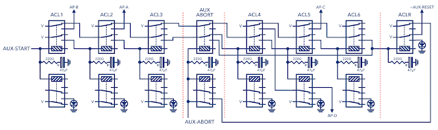
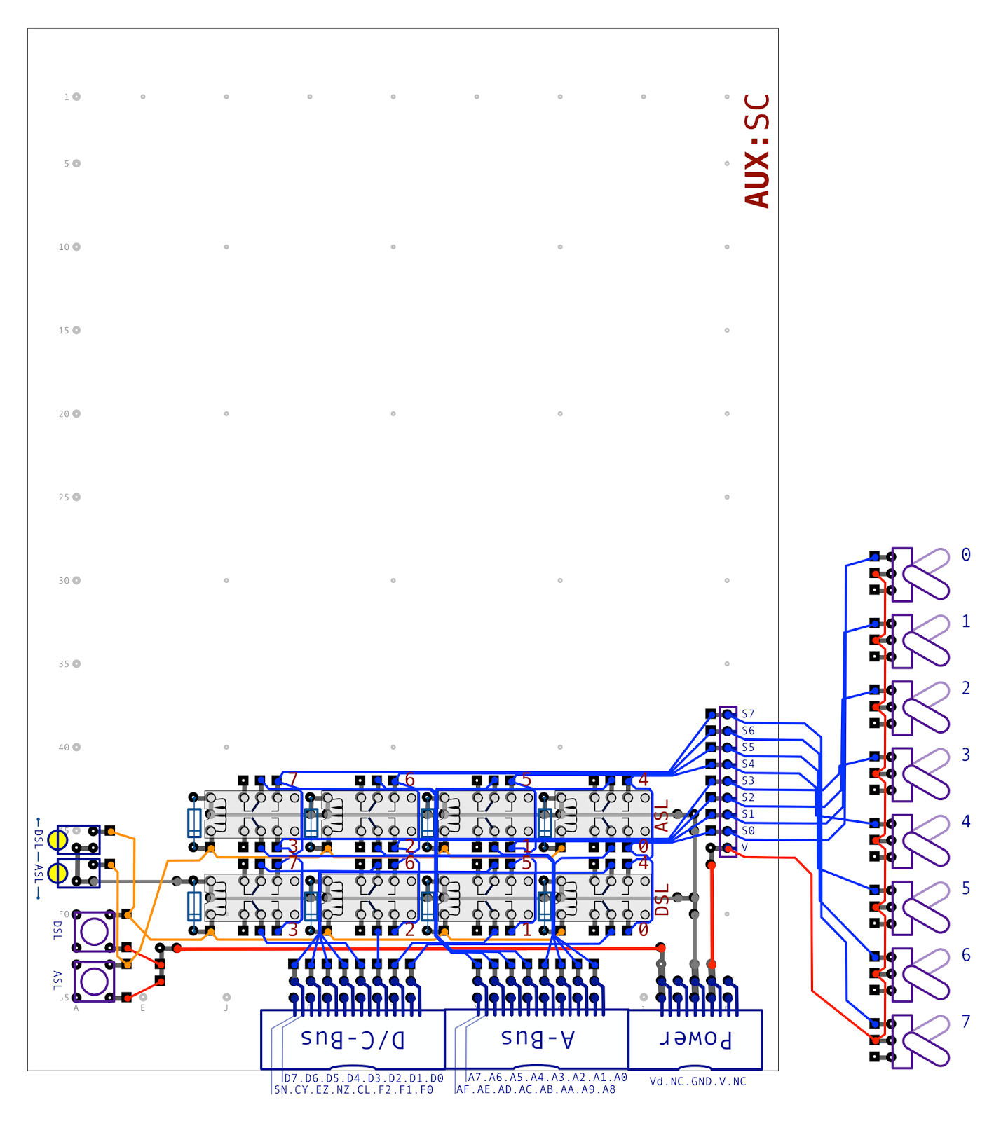
This is the last post in a mini-series of three covering the design of the auxiliary control unit which will ease entering and inspecting programs in the computer’s memory. In my last post I covered the design of the auxiliary clock which resulted in the following schematic:
… which generates the following timing pulses …
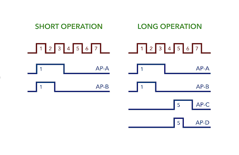
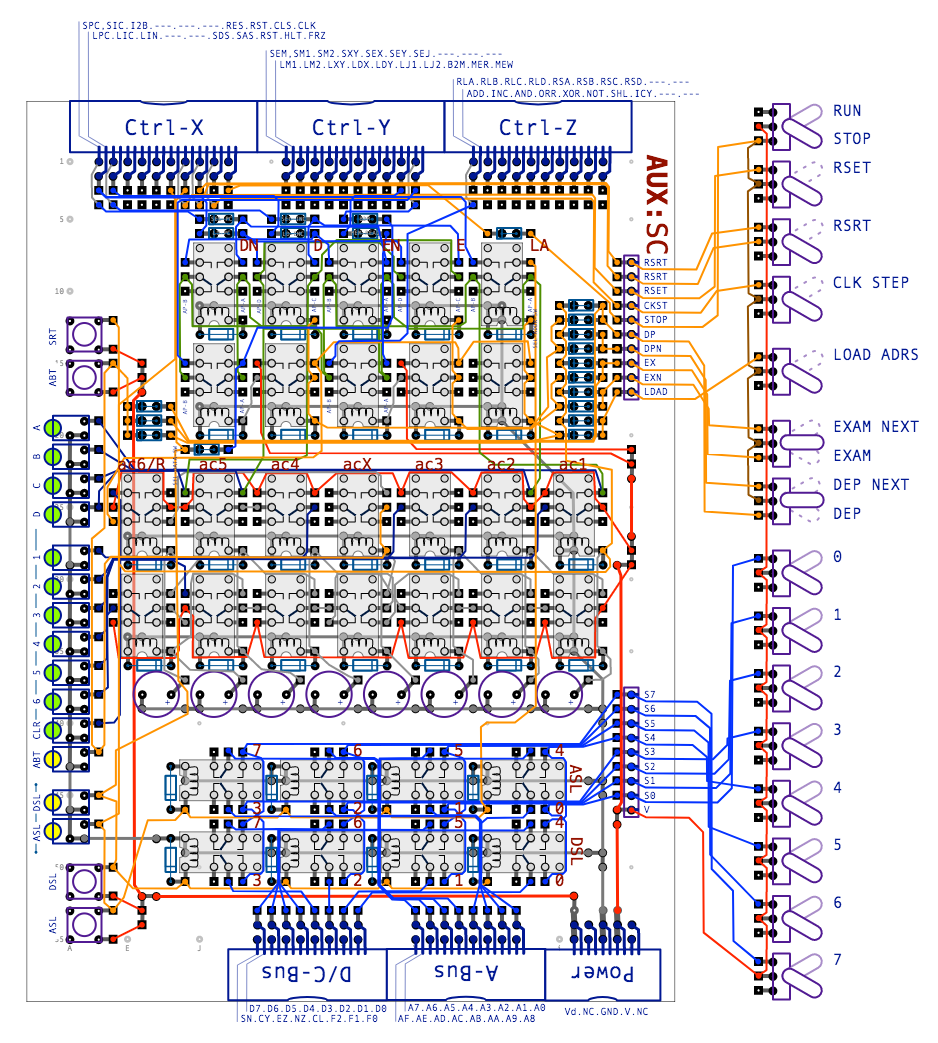
This post covers the last part of the puzzle which is designing the control logic that will take the pulses above and use them to drive the appropriate control lines at the right time according to the instruction the user requested as follows:
OK, let’s get started … first thing I want to do is start the auxiliary clock whenever an instruction is requested via the user flicking one of the primary switches. That’s easy enough … just activate the AUX-START line shown in the schematic above … but … we mustn’t back-feed any of the other instruction types so some diodes are needed:
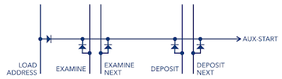
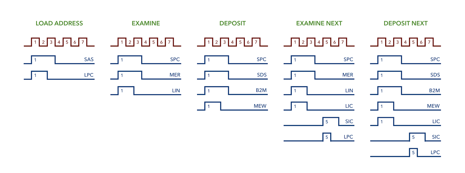
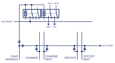
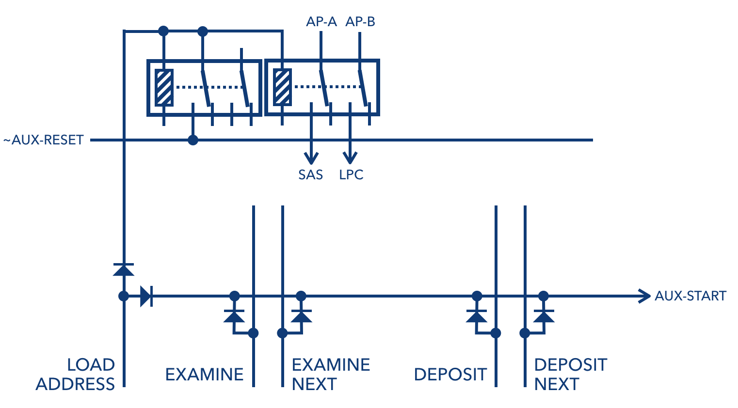
Next we can add the control logic for ‘LOAD ADDRESS’ which is a relatively easy one as it only hits two control lines: Select Address Switches (SAS) and Load Program Counter (LPC):
One thing worthy of mention here is the presence of the AUX-RESET which latches the control relays on following the activation of the ‘LOAD ADDRESS’ line which is momentary as the switch is spring loaded to return to it’s neutral position. When the auxiliary clock finishes its sequence the AUX-RESET line is dropped which in turn un-latches the control relays ready for the next instruction.
Before continuing on with the other instructions let’s pick off the ‘NEXT’ handling which will load the program counter (LPC) from the incrementer (SIC) on timing pulses C and D:
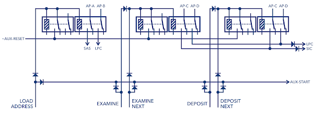
The pattern is very similar to the ‘LOAD ADDRESS’ operation although note that on the LPC and SIC lines we don’t need to stop the ‘DEPOSIT’ relays back-feeding the ‘EXAMINE’ relays as they’ll never be active at the same time but we do want to stop the rest of the computer back-feeding these lines and so the diodes are placed at the point the lines leave this unit. Note also that all of the remaining functions are activating their set of relays whether they’re ‘NEXT’ functions or not. This is fine as AP-C and AP-D only fire on a long instruction … however … we haven’t told the auxiliary clock yet whether it is in fact a short or a long instruction we’re doing. We can fix that though by setting the AUX-ABORT line:
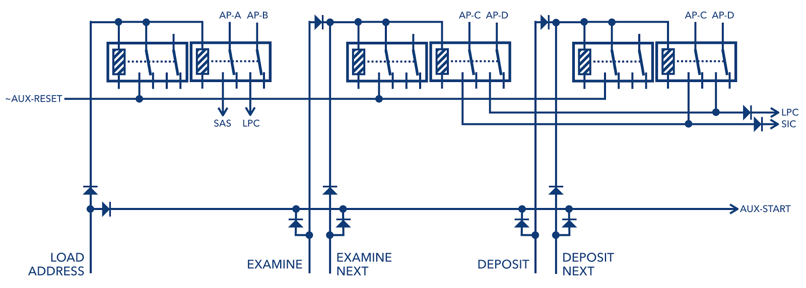
All of the short instructions will now activate the AUX-ABORT line meaning the auxiliary clock will only produce pulses A and B. We can now move on to implementing the ‘EXAMINE’ and ‘EXAMINE NEXT’ instruction handling:
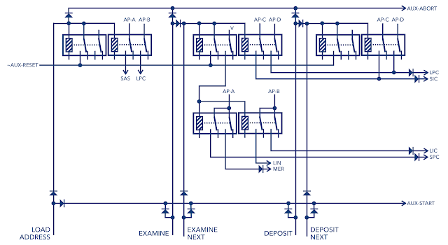
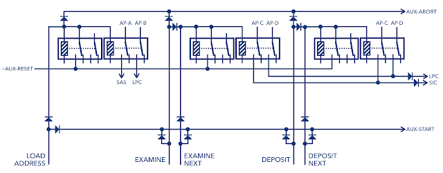
You might have spotted there that we’re firing the LIC line for both ‘EXAMINE’ and ‘EXAMINE NEXT’ even though it shouldn’t be fired for ‘EXAMINE’ function. This has been done to simplify the circuitry here at the expense of performing an unnecessary action. Let’s finish off with implementing the ‘DEPOSIT’ and ‘DEPOSIT NEXT’ instruction handling:
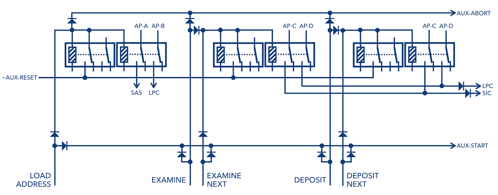
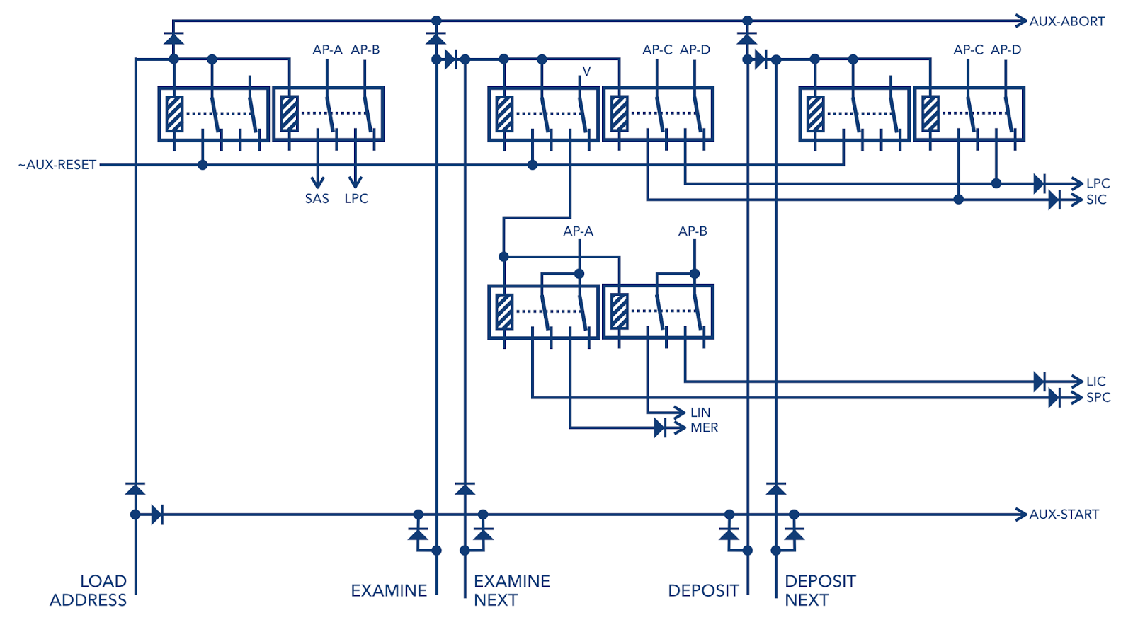
With those last instructions implemented the schematic above is completed and we can now combine that with the auxiliary clock schematic shown at the top of this post. Returning to my usual diagram style here is the auxiliary card as it currently stands:
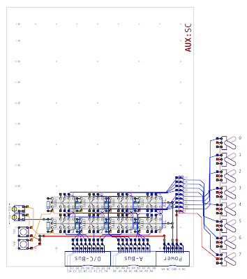
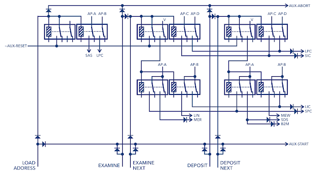
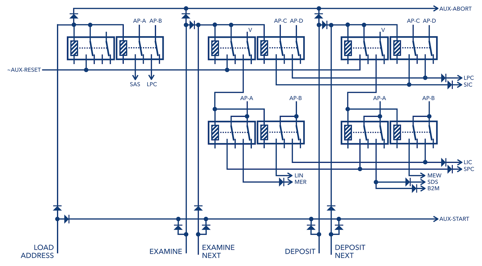
… and here it is with the auxiliary clock and control relays added:
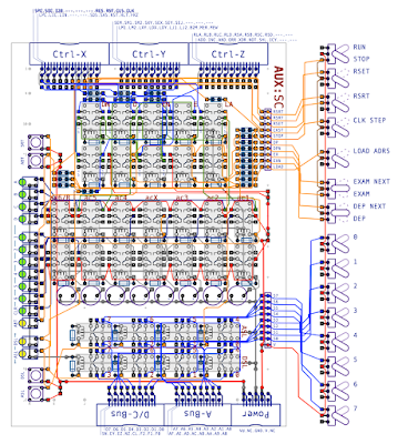
The auxiliary clock relays are in the middle of the card and the control relays covered in this post are towards the top. As always, you can find a larger version of this card design here in PDF format.
So, with the auxiliary control card design in the bag it’s time to whip out the soldering iron again and get constructing and I’ll cover that in my next post.