In my last post I made a start on the memory unit construction with the lower memory card. The lower card centres around the memory IC which runs at 5V. The upper memory card picks up the task of converting the data and address bus coming in from the rest of the computer (running at 12V) to the 5V needed by the memory IC.
The LEDs and backplane connectors were soldered down in my last post so we can jump straight to adding the card interconnects which pass the local address/data busses to the lower card:
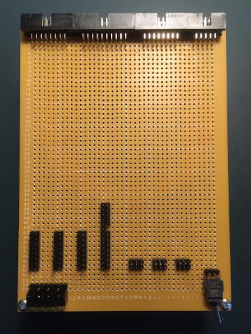
These interconnects mate with the matching sockets on the lower card and when sandwiched together the two cards form the memory unit.
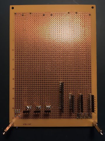
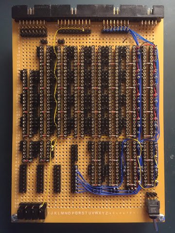
Next job is to solder down all the relay sockets and wire wrap posts. In my last post I mentioned that the upper memory card is quite densely populated as a large number of relays are required to handle all the data and address bus conversion. On previous cards I’ve soldered down two rows of turned pin sockets with the wire wrap posts alongside for each and every relay. On cards such as this it does become a bit of a fiddly and tedious job and so I’m changing approach this time and having a go at soldering down whole rows of connectors for a group of relays. Here’s what that looks like:
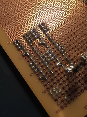
As you can probably see this is slightly wasteful in terms of unused sockets and pins (and therefore increases the cost slightly) but I’ve offset that against the time it takes to construct. In theory my time is free but my patience isn’t and given this is ultimately a hobby it’s quite right that I should look for more efficient ways of doing things to save boredom setting in. I can repeat this pattern to get the rest of the relay sockets soldered down:
You may have noticed that there’s no gaps left for the diodes that sit in front of each relay and that’s because they’ll be popped in to the sockets as well - again this simplifies the soldering. Looking at the picture above left you can also see there’s a break in the rows about two fifths up the card and that’s intentional so that the wire wrap can run across the card horizontally where needed.
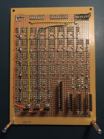
On the back of the card (pictured above) you can also see another alternative approach - this time in how I’m constructing the ground lines. On previous cards I’ve used insulated wire that needs individually cutting, trimming and soldering down. Again, that’s a time consuming (and increasingly tedious) job and so it’s ripe for a change of approach. So, this time around I’ve soldered bare wire down right across all the points that need it. This is much quicker but does run the risk of shorting something out although once soldered down those wires aren’t going anywhere so the risk is pretty minimal. All other power lines still stick with the insulated wire as they cross ground wires in many places. Note that on this card there are two power lines: the red 12V line and the yellow 5V line.
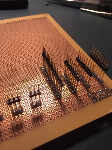
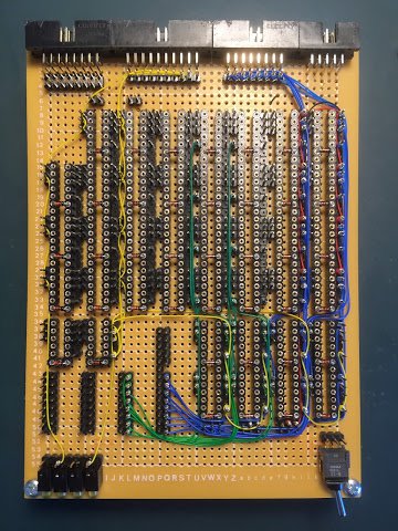
With all the soldering in place it’s time to move on to fitting the diodes and making a start on the wire wrap:
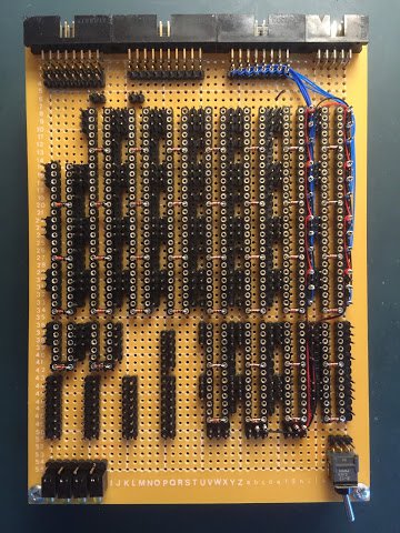
You can now see how the diodes fit in which would make replacement easier in the (very) unlikely event of a component failure. The first round of wire wrap here brings the data bus in to the conversion relays such that when a line of the bus is connected to 12V the relays connect the output to 5V and when a line of the bus is disconnected from 12V the relays connect the output to the 5V ground. Let’s complete the incoming data bus wire wrap:
The converted inbound data bus lines are now routed through a set of gating relays so that it’s only connected to the internal memory bus when we need it … and ‘when we need it’ is determined by the ‘Bus To Memory’ (B2M) control line seen here in yellow. Similarly we can now wire up the output data bus:
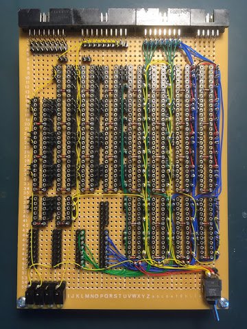
This time the green wire wrap comes off the card interconnects and sends the outbound memory data bus through a set of gating relays. This time we’re only gating those lines when the memory is being read. The control wiring is set up such that B2M is vetoed when the MR (memory read) line is active. The outbound memory data bus is unusual in that when a bit is set in memory the according bus line is grounded (and is held high otherwise) due to the way the relay driver IC works on the lower card. This means that we connect the negative side of each relay to this data bus and the positive side to 12V (via the memory enable switch). From those ‘conversion’ relays it’s straight out to the computer’s data bus.
Last wire wrap job is to hook up the computer’s address bus to the local memory address bus:
This is very similar to the incoming data bus wire wrap in that we convert the connected/disconnected 12V to 5V power/ground. This time though no gating is required as the address bus is permanently connected to the memory chip and is effectively ‘read only’. Note that there are only 15 relays because the last bit of the address bus is used to select the memory unit … when unset the memory unit is active and when set the memory unit effectively disconnects from the computer. This way you can address the full 32,768 slots of the memory chip whilst leaving another 32,768 slots available for future expansion. That ‘future expansion’ doesn’t have to be more memory by the way … it could be a display unit or similar.
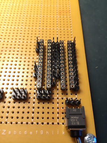
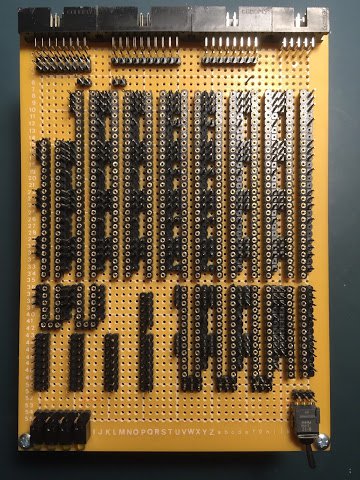
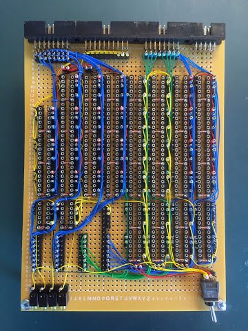
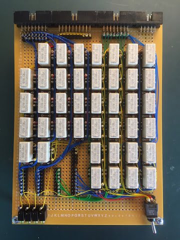
Right, let’s pop the relays in and the upper memory card is complete:
In my next post I’ll connect the upper and lower cards together thereby forming the memory unit as a whole and give it all a test.