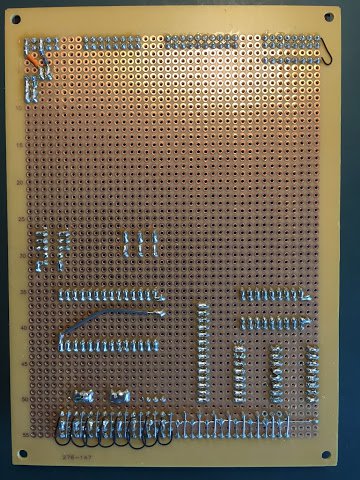
It’s time to make a start on the construction of the memory unit and as mentioned in my last post this one is a bit more complex than ‘boring old registers’ and so I’ll split it over two posts. Let’s dive in with the easy part - soldering down the LEDs and backplane connectors:
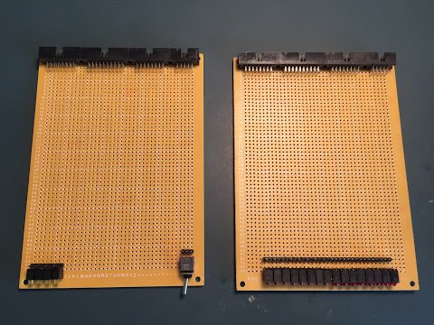
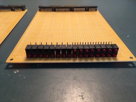
For the lower memory card there are 16 LEDs for the 16-bit address bus and 8 LEDs for the 8-bit data bus. Both of these busses are ’local’ to the memory unit and operate on +5V and ground as covered in my post on the memory unit design. Unfortunately I’ve messed up here a bit as I’ve merrily gone and soldered down the same LEDs I use on all the other cards … the 12V ones. Although these LEDs will work with 5V they won’t be as bright due to the internal resistor in each being rated for 12V operation. A bit of a silly mistake to make but it’s done and I’m not so upset by it that it’s worth changing them over … I only realised when I tested the card and noticed the LEDs weren’t as bright as usual (doh).
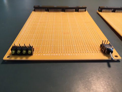
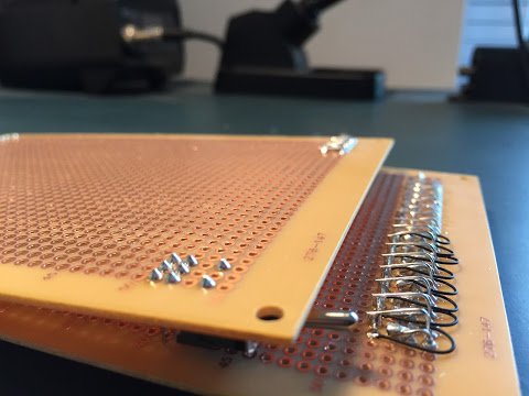
The upper memory card has four LEDs on the left which show what the memory unit is up to and the switch on the right disconnects the memory from outputting to the data bus which comes in handy when debugging. Here’s a close up of the cards from the rear:
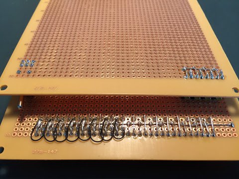
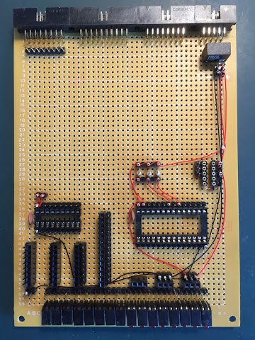
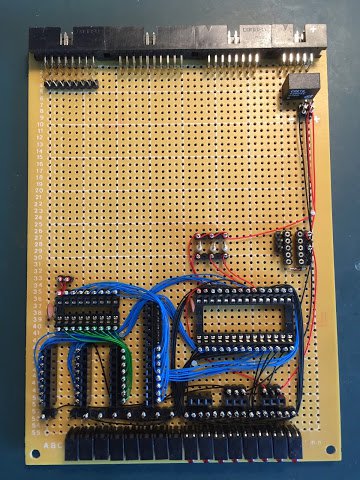
Right, I’ll leave the upper card there for now and pick it up in my next post. Focussing on the lower card then let’s add some sockets, board interconnects and wire wrap posts:
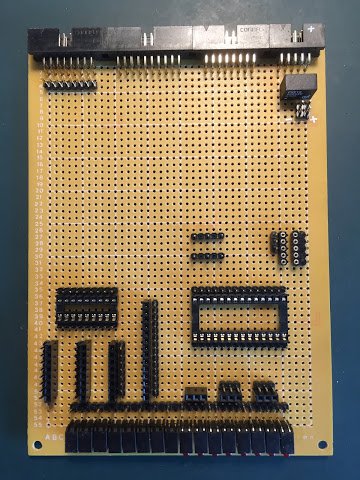
Nothing too unusual there - larger IC socket for the memory chip, smaller one for the relay driver. The interconnect sockets will mate with the equivalent on the upper card to pass the memory address and data busses through. There’s only one relay in this card (something that definitely can’t be said for the upper card) and so accordingly only one relay socket is needed. In the middle right of the card there’s two rows of posts which is where the pull up resistors will go and finally at the top right the DC/DC convertor is soldered in which will take the usual 12V used elsewhere in the computer and step it down to 5V which is needed by the memory IC. This does mean, of course, that there’s four power lines going on (+12V, 12V ground, +5V and 5V ground). Moving on, let’s add the diodes, resistors and caps:
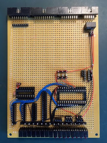
The diode is the usual flyback that goes across each relay in the computer to ‘soak up’ the voltage spike caused when the relay coil is turned off. The resistors are used to pull up some of the memory chip control lines so that they stay in that state unless we ground that line intentionally to activate it. For the memory chips the control lines operate in reverse to how you’d expect … so output enable is active when grounded but disabled when held high. Finally there’s two decoupling capacitors sat next to the IC sockets to filter out any noise on the circuit.
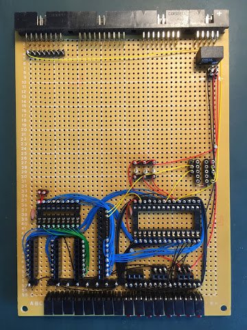
Last bit of soldering to do is the power rails:
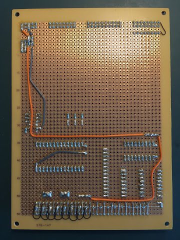
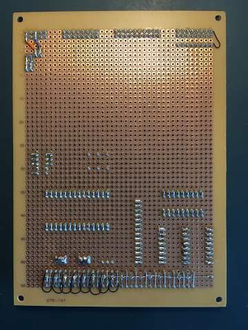
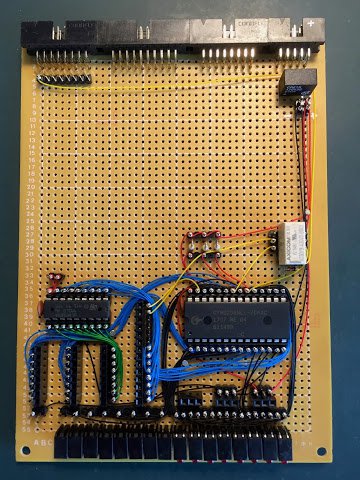
… and then it’s on with the wire wrap …
Starting with the first picture the 5V power and ground lines are wired out followed by the data and address bus lines in blue. With that done the third picture shows the data bus out lines which come off the relay driver socket in green and then finally it’s the yellow control lines. In this case there’s only one control line which comes off the last bit of the address bus to enable/disable the memory unit as a whole. With that in place it means if we wanted to use the upper 32K address space for something else later on the memory unit won’t interfere - its only interested when we’re addressing the lower 32K address space.
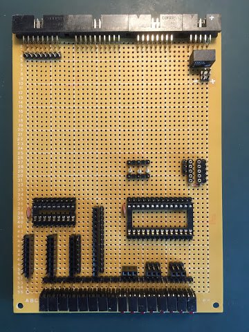
Last job then is to pop in the ICs and the single relay and that’s the lower card done:
In the next post I’ll construct the upper memory card which will have a lot more relays on it and be far more densely packed.