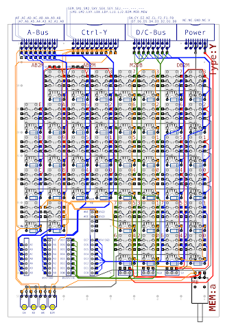
In my last post I started the design for the computer’s memory unit which is spread over two cards. With the lower memory card design in place its now time to finish the job and design the upper card which will interface the rest of the computer with the memory chip of the lower card.
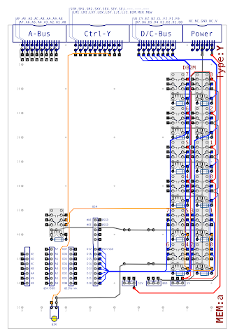
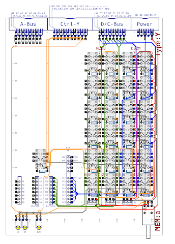
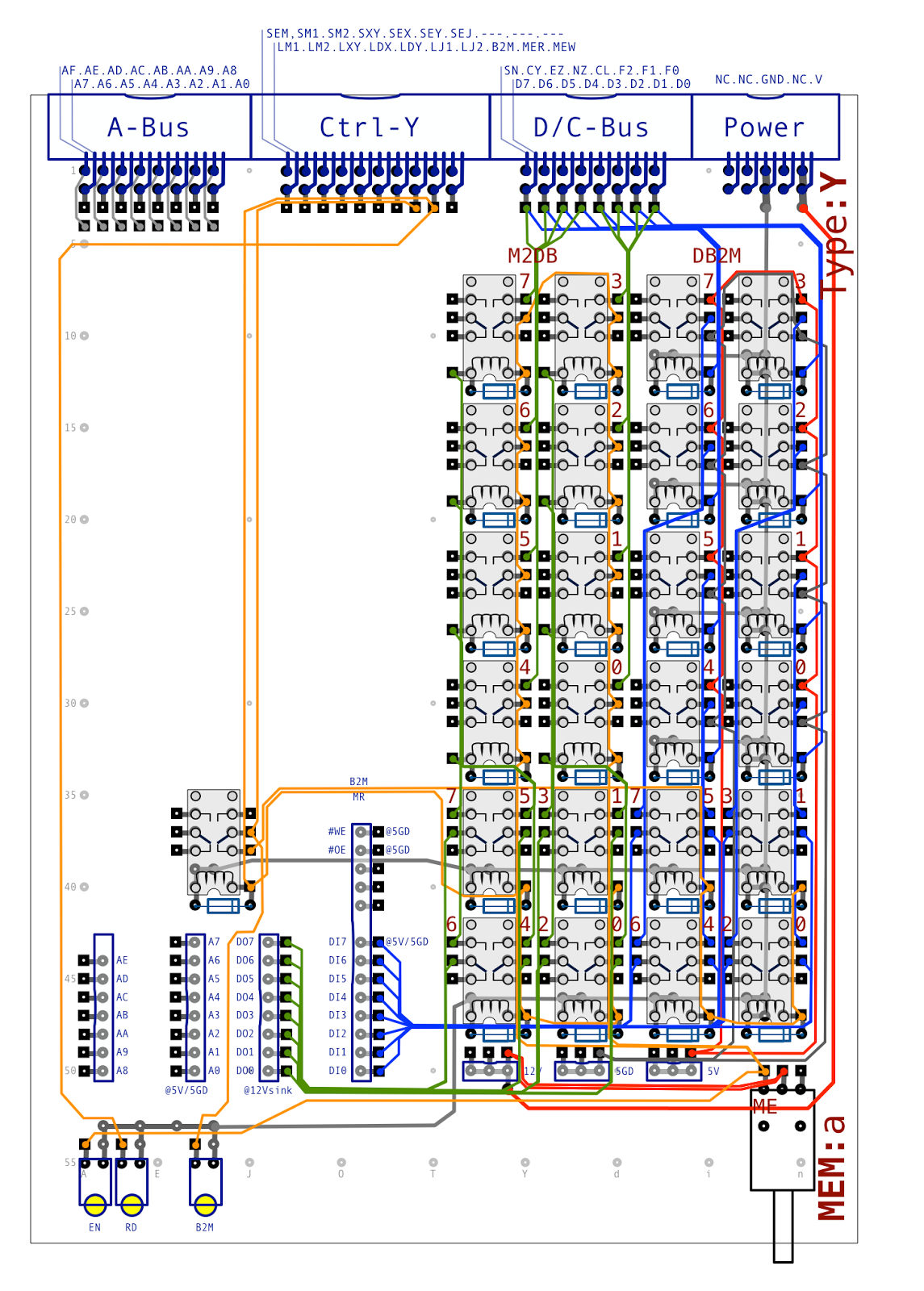
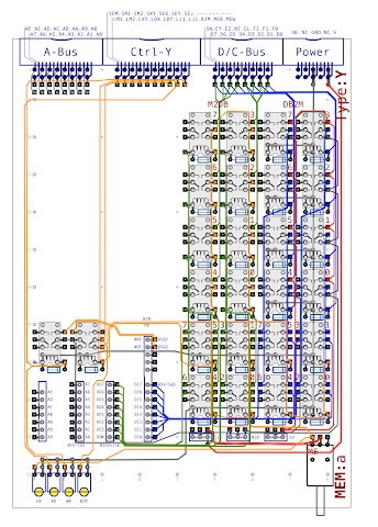
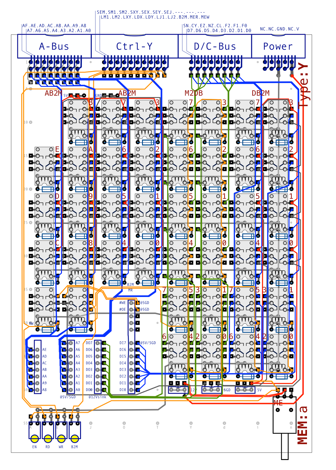
Let’s dive straight in by bringing up the board interconnects from the lower card:
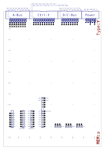
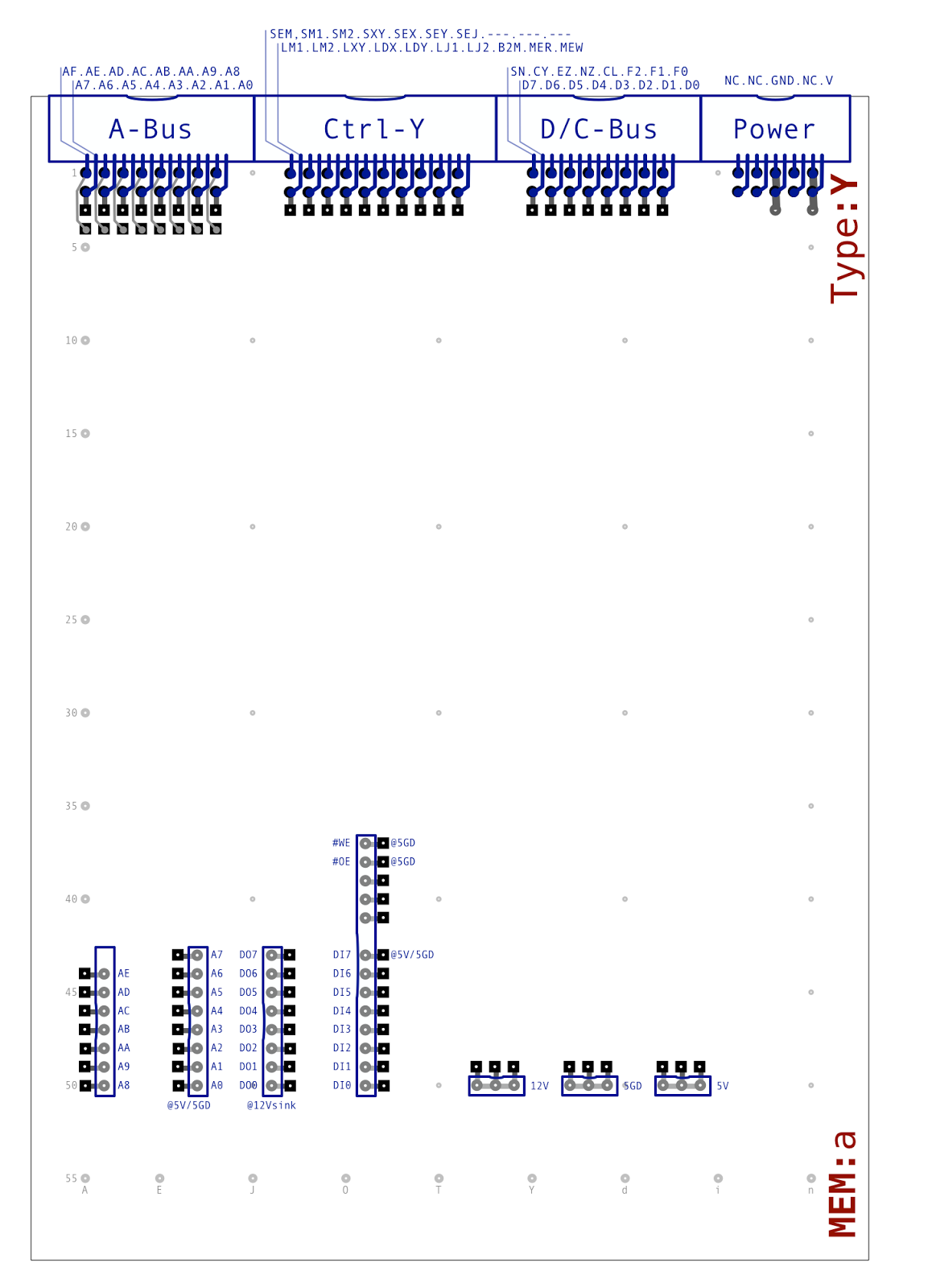
The left two columns bring up the address bus for the memory chip which needs to be at 5V for a logic 1 and at ground for a logic 0. The third column brings up the outbound data bus which will sink 12V to ground for a logic 1 but holds at 12V for a logic 0 (effectively an inverse of what you’d expect). The fourth column brings up the inbound data bus which takes 5V for 1 and ground for 0 along with the write enable (WE) control line and output enable (OE) line which work in reverse (5V for disabled and ground for enabled). The last three connects to the right are power at 12V, ground for 5V and finally 5V. As you can probably guess there’s going to need to be quite a lot of ’translation’ logic on this card.
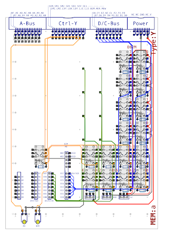
First ’translation’ job is to take the computer data bus, which is 12V for a logic 1 and disconnected for a 0, and wire that out to 5V for 1 and ground for 0. That’s not overly complicated and looks like this:
Note that although we now have the data bus converted to something suitable for the memory chip we need to be able to gate this so it’s only connected when we’re storing a value to memory. This is because when we’re reading a value it comes back in through the outbound data bus interconnects. With the additional gating added the card looks like this:
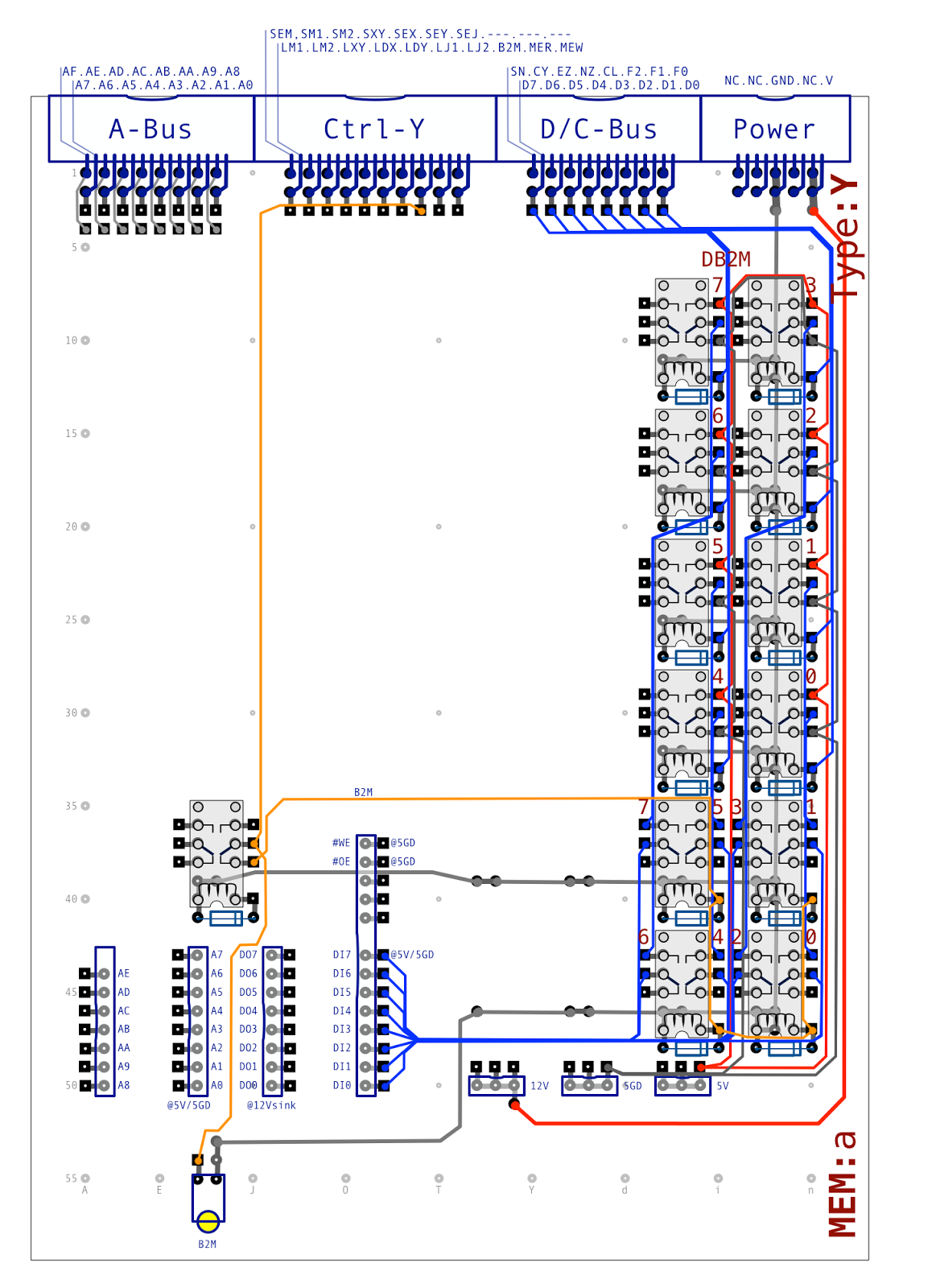
The line that controls the gating of the inbound data bus is named ‘B2M’ which stands for ‘Bus To Memory’ (because that’s what it does). There’s a ‘veto’ relay on the control line which will be used later on to override the B2M line when required.
Let’s turn now to the data bus feed coming back from the memory chip which will also need gating so that it only influences the data bus of the computer when needed:
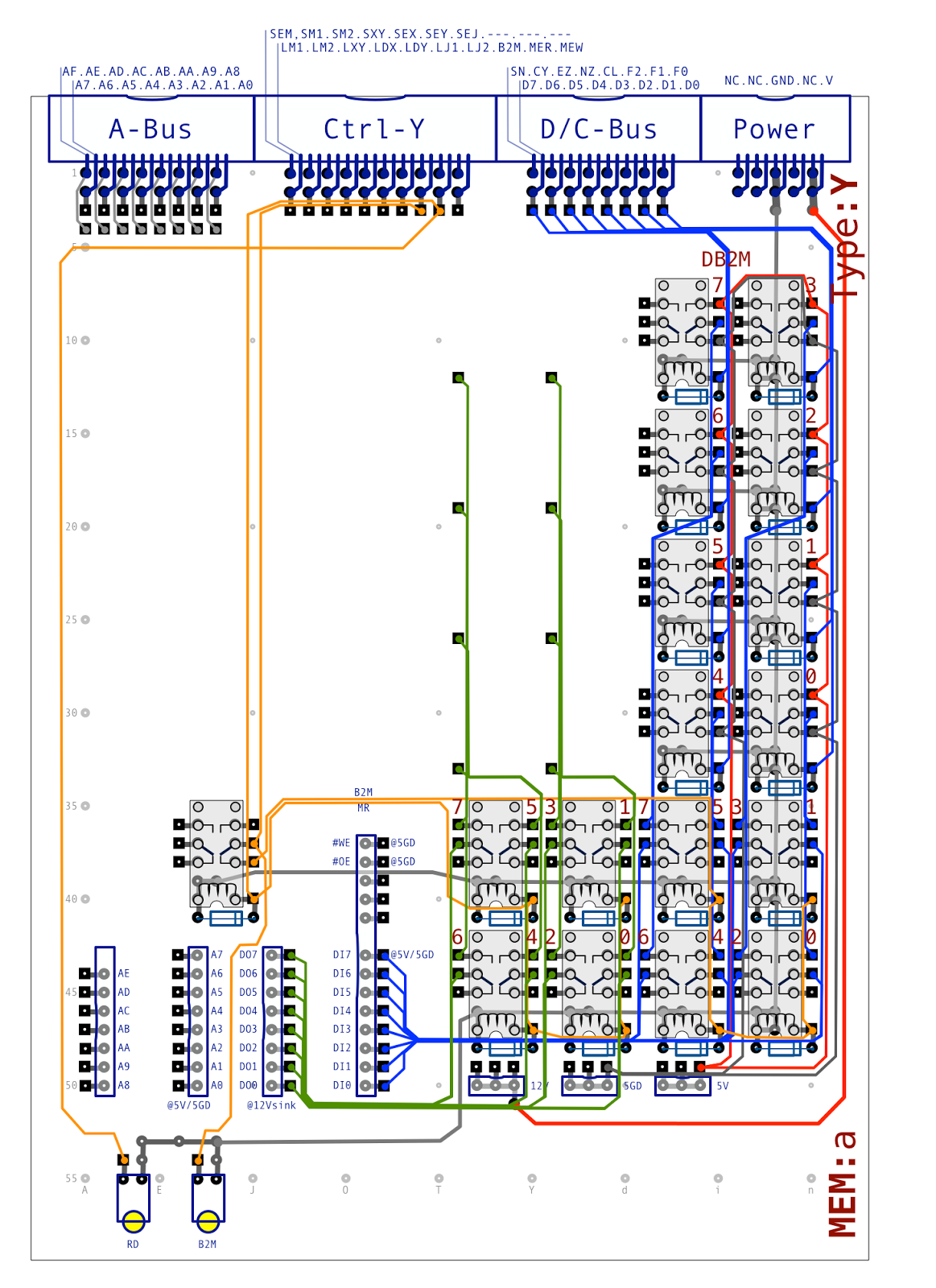
The memory read (MR) line controls these particular gating relays but also the B2M ‘veto’ relay to ensure that if we’re reading a value from the memory chip we can’t be loading it at the same time. Without this we could have odd situations where a 5V coming off the memory chip is shorted to ground on the input bus.
To get the memory value all the way out to the computer data bus there’s a bit more translation required. In this case if the memory chip is putting out 5V on a line the relay driver will sink 12V to ground whereas if the memory chip is at ground on a line the relay driver will hold at 12V (logically inverted). To make this work this is the only place in the computer where we play with the ‘other’ side of the relay coil (which is usually soldered to ground):
On the positive side of the relay coils we extend the MR control line so that the relays only operate whilst MR is held high. The negative side of the relay coils are connected, via the gating relays, to the relay driver on the lower memory card. Therefore, it takes the MR line to be high and the data bus line to be sinking to ground for the relay to switch on. Whilst the relay is switched on it’ll gate the MR line to the appropriate bit of the data bus creating the end result that we’re after.
The final part of the data bus ‘picture’ is to operate the write enable (WE) and output enable (OE) lines of the memory chip which as mentioned earlier operate in reverse of what you’d expect: 5V to disable and ground to enable. Only one additional relay is required:
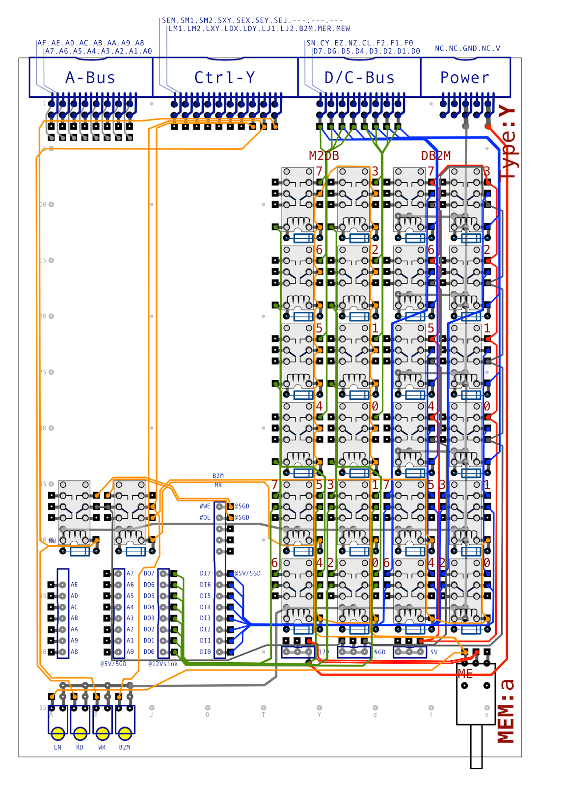
The OE line is grounded whilst the memory read (MR) line is high but disconnected otherwise. That’s fine in this case as the line is pulled to high via a resistor on the lower memory card. In other words the output is disabled by default until requested by the MR line. There’s an additional control line introduced above which is the memory write (MW) line. The MW line pulls the write enable (WE) line low when MW is high. Again the WE line is pulled to high via a resistor on the lower memory cards and again the WE is disabled by default until requested by the MW line.
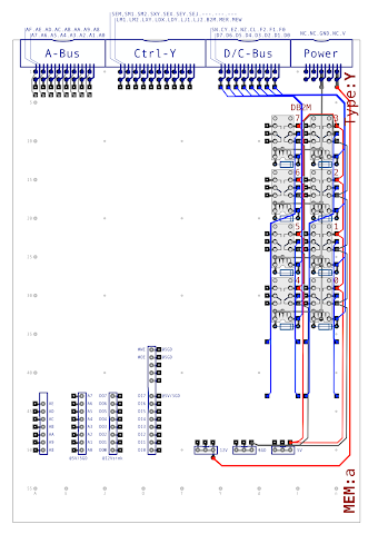
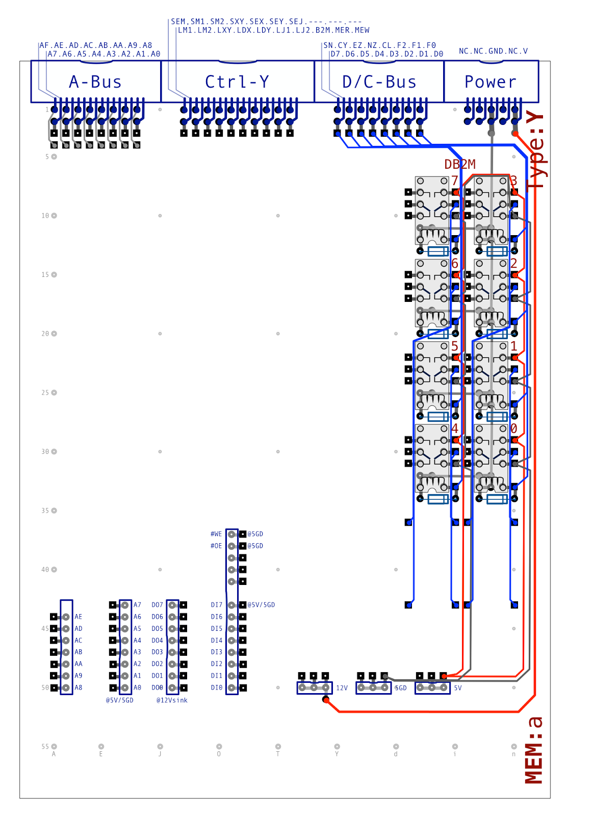
That completes the data bus wiring but seems a shame not to fill the remaining space of the card with yet more relays so let’s go for that:
The final relays above translate the incoming address bus, at 12V for 1 and disconnected for 0, to the required 5V for 1 or ground for 0. In this case no gating is required as it’s no problem having the memory card always reacting to the current value on the address bus … well, except for the extra power consumption of firing relays unnecessarily perhaps. Notice that there’s only 15 address bus relays even though, of course, there’s 16 lines on the address bus. As mentioned in the last post we’re dealing with a 32K memory chip and therefore only use half the addressable space which leaves room for future expansion in the upper addressable space.
So, that’s ended up as one of the ‘busier’ card designs in the computer and it’s one where I’ll need to be careful with the wiring when constructing. Nonetheless that’s the memory unit design complete and ready to go and as always you can find a version here in PDF format.
With the memory card, program counter and incrementer design in the bag we’re very close to having a computer that can run a program in memory. In the next post I’ll cover the final piece of the puzzle which is to update the controller card to orchestrate using these three units together.