In my last post I explained my decision to use a ‘modern’ memory chip in my relay computer … I also alluded to there being some complexities in interfacing the rest of the computer with that memory chip. The memory unit will be spread over two cards and in this post I cover the design of the first half and expand on those ‘complexities’ a bit.
The memory chip I’m using is from the ‘62’ family of CMOS 256Kbit (32K x 8) Static RAM … effectively meaning it can store 32,768 separate 8 bit values referenced by a 15bit address bus. Buying chips can be a bit of a ’needle in a haystack’ when you’re buying through one of the larger electronics suppliers (I use Mouser). Knowing the chip number isn’t enough to actually buy one and doing a search on Mouser for ‘62256 memory’ narrows it down to 61 matches. I can narrow it down further as I know I need through-hole mounting (not surface mount) and that gets me to 6 matches. Next choice is access speed … 55ns or 70ns. This is actually a bit of a mute point for this computer as it’ll get nowhere near that speed (the relays take around 5ms to switch) so lets ignore that one. So faced with 6 choices it comes down to price and what’s in stock. In the end I went for a mid-priced chip from Cypress Semiconductor … a CY62256NLL-70PXC for £2.77 (‘cheap as chips’ … literally).
CY62256NLL-70PXC … catchy name eh?! There’s a data sheet for the chip here but effectively the code is telling you it’s from Cypress Semiconductor [CY]; it’s the 62 family of CMOS 32K SRAM chips (256Kbit) [62256]; it’s using a Nitride Seal Mask fix [N]; it’s low power [LL]; access time is 70ns [70]; packaged in a 28-pin moulded DIP [PX]; and finally it’s the commercial temperature grade [C] that’s happiest between 0 and 70 degrees centigrade.
What’s quite nice with these 62256 chips is that you can pair two of them up together sharing the same data and address bus and then use the most significant bit of the address bus to enable one chip and disable the other. With that set up you get the full 64K memory for your 16-bit address bus. As mentioned in my last post though I’m not going with that solution and I’m sticking with one 32K chip and using the remaining address space for ‘future expansion’.
Right, so back to that ‘complexity’ (no, buying the right chip wasn’t the ‘complex’ thing). CMOS chips have some interesting properties but the one to definitely watch out for is making sure that any inputs are connected to voltage or to ground - never left unconnected. This is because the inputs have very high impedance (resistance) which is good because it means they will not affect the part of the circuit where they are connected. However, it also means that unconnected inputs can easily pick up electrical noise and rapidly change between high and low states in an unpredictable way. This is likely to make the chip behave erratically and to prevent problems all unused inputs absolutely must be connected even if it’s a part of the chip that’s not being used (which can be tempting with chips that have multiple logic gates).
Why am I picking that out specifically then? Well, the computer operates by connecting and disconnecting power via relays which means that a line coming from a relay that’s turned off is disconnected (not wired to ground). It’s floating and for a CMOS chip that means erratic behaviour. To make this all work I’m going to have to do some clever relay work to ensure the memory chip is always connected to power or ground. Oh … did I also mention the chip works on 5V not the 12V the rest of the computer uses? That means there’ll be two levels of voltage running around the card and though the lines which’ll all need careful planning. Anyhoo, let’s make a start.
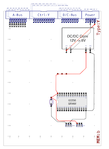
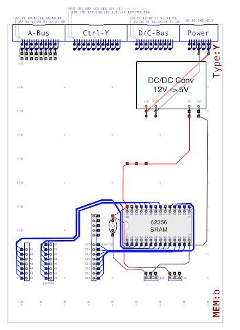
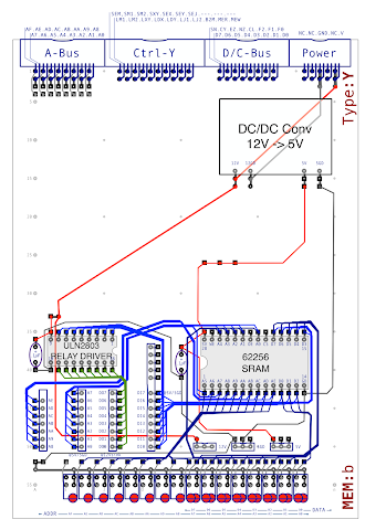
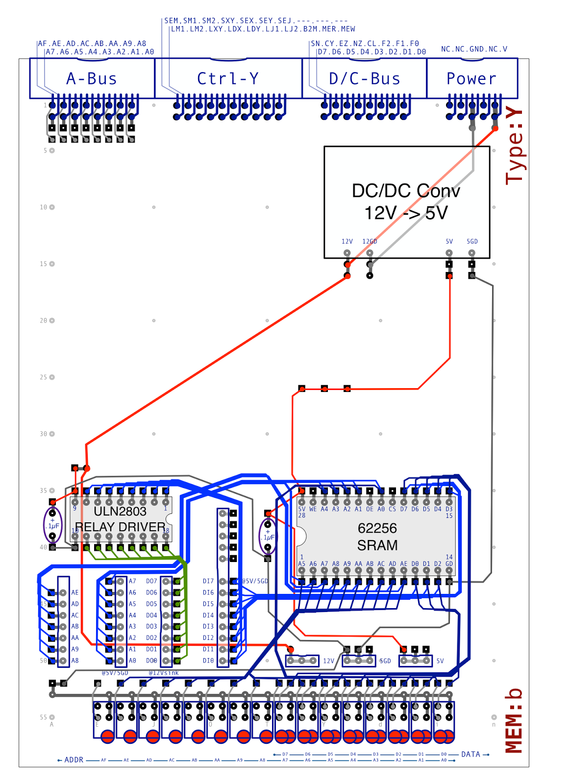
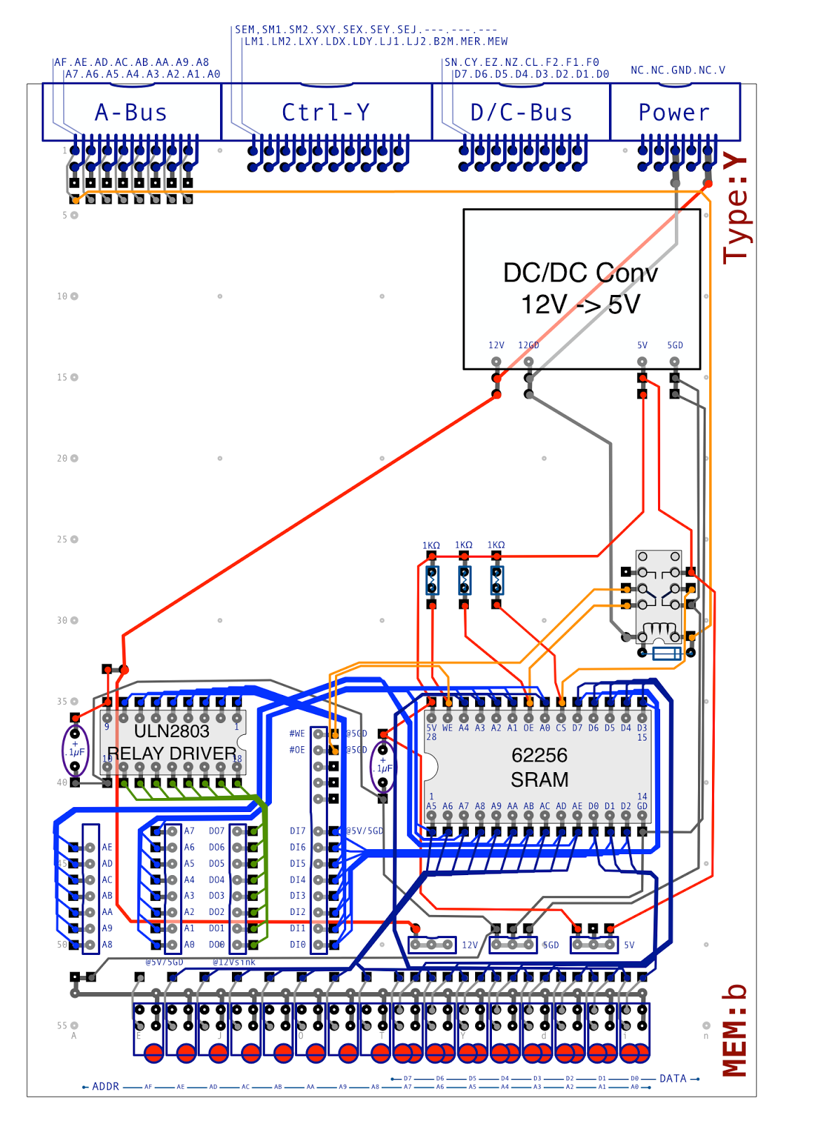
First things first let’s get the memory chip on to the card and to power it I’ll add a DC/DC convertor which will drop the 12V down to the 5V the chip needs:
At the bottom of the card there are board interconnects for the 5V and ground coming out of the DC/DC convertor which will pass through to the other memory card and are used as needed (which will be discussed in my next blog post). Also worthy of note is the 0.1 micro farad capacitor to the left of the CMOS chip. This is a decoupling capacitor and works best when placed as close to the chip as possible.
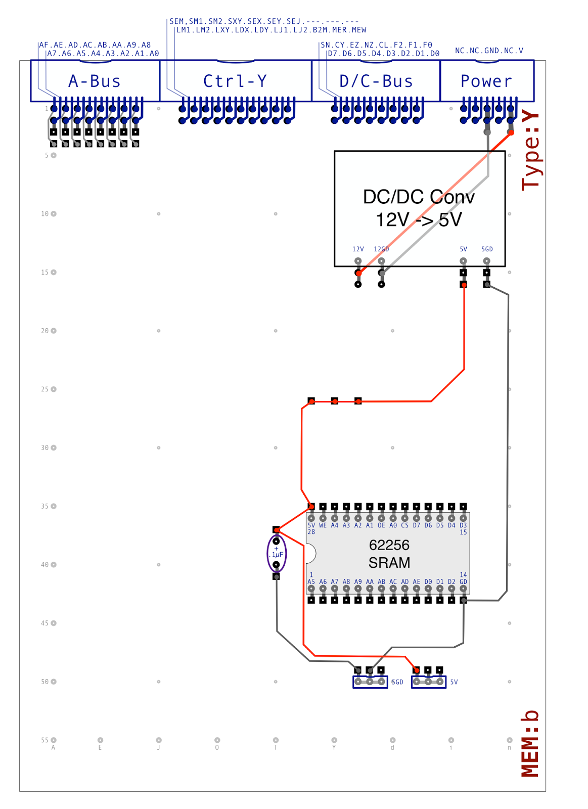
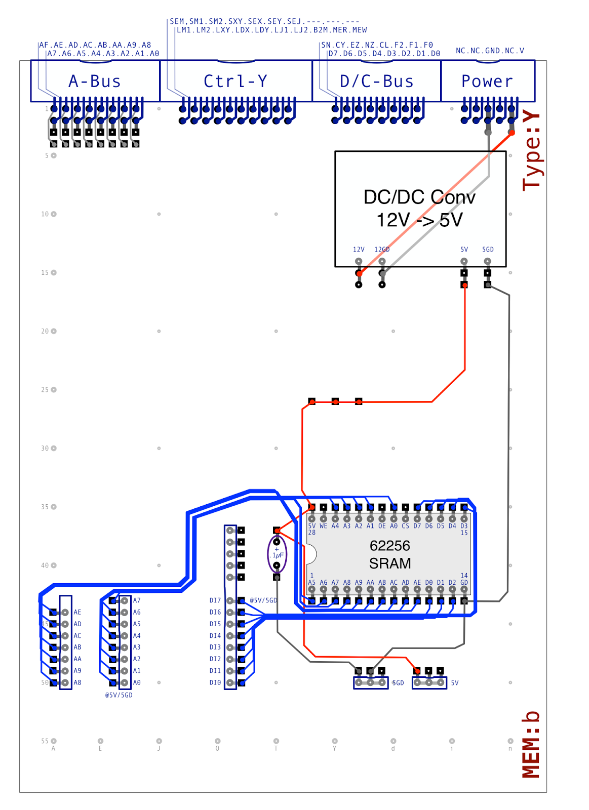
I can now start wiring the memory chip out and I’ll start with a easy one … the address bus:
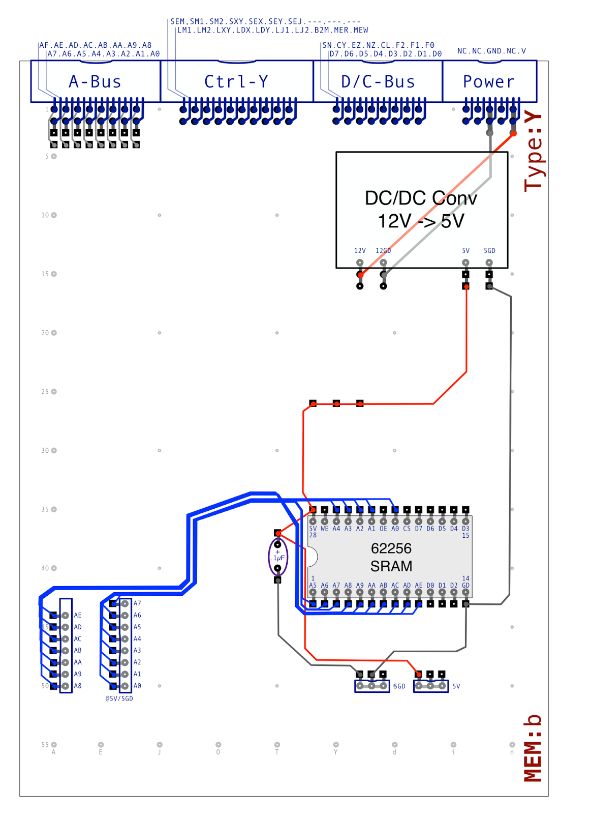
As mentioned earlier these bus lines must be connected to either +5V or ground representing a binary 0 or 1 respectively. The responsibility for this is handed off to the other memory card via the board interconnects. Note that there’s only 15 bits connected (to address the 32K locations). I can now move on to the data bus:
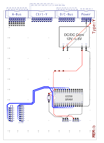
As with the address bus these data bus lines must be connected to either +5V or ground. You can probably work out that the address bus is ‘read only’, that is, the chip never sets a value on the address bus. What maybe isn’t so obvious is that the data bus here is also ‘read only’. We’ll see why shortly but in the meanwhile given we’ve got address and data busses down lets add some LEDs:
There’s nothing too surprising there … the usual LEDs … however it’s worth noting that we’re running the LEDs on 5V this time around rather than the usual 12V. Actually, this is something that totally passed me by when I designed the card and ordered the parts so I’ve ended up with yet more 12V LEDs. They’ll work on 5V but won’t be as bright as all the other LEDs in the computer … annoying but not the end of the World.
Anyhoo, back to that data bus … the memory chip can read from the data bus or write to it depending what you ask for. When we’re doing a read operation we need to drive the main data bus of the computer which runs at 12V. We’ve only got 5V running on our ’local’ data bus however so there’s an extra bit of wizardry required:
Here I’ve added a ULN2803 darlington transistor array (data sheet here) to react to the 5V data bus and drive out 12V on the other side. This is quite a nicely laid out chip with each input having its corresponding output on the opposite side. There is, however, a bit of a quirk with this chip which means that a high value on the input creates a low value on the output and vice-verse … effectively inverting the input. It’s not really a quirk of course, just the way the design works, but that’ll need wiring out on the other memory card.
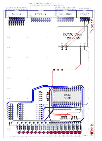
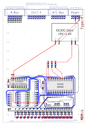
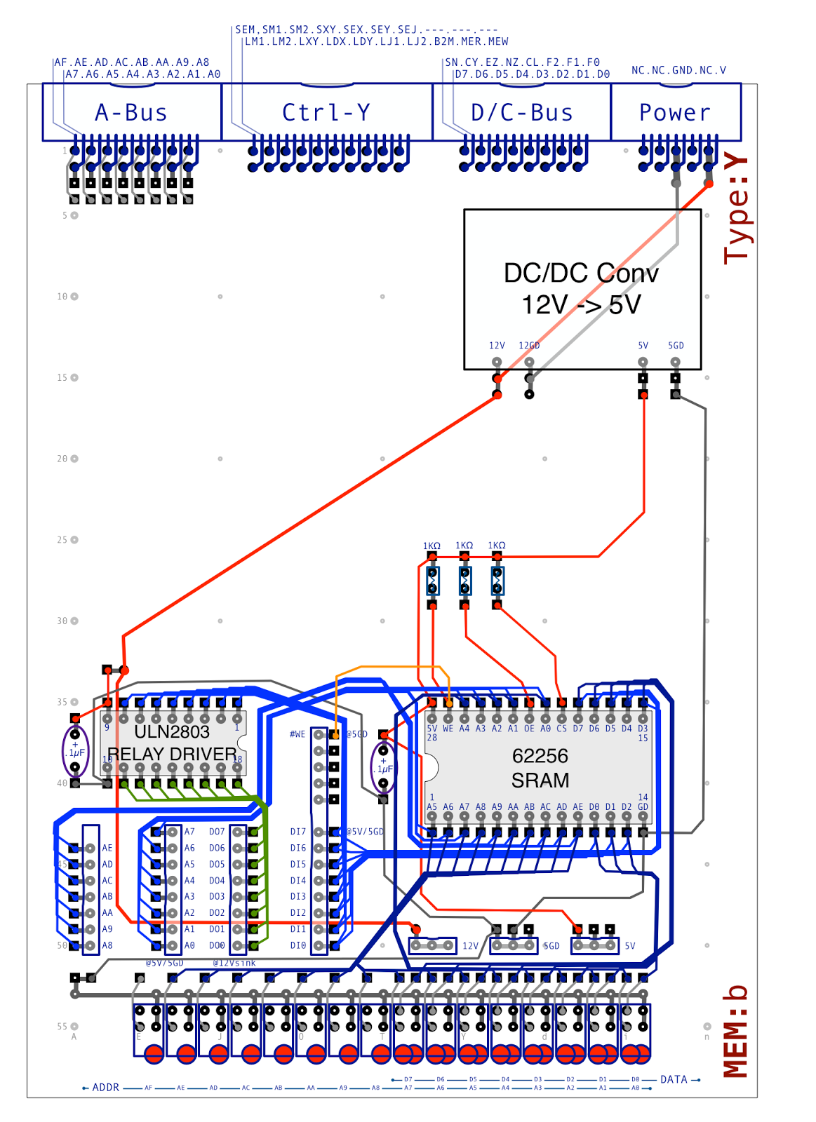
Nearly there now. Let’s start adding some control lines:
First of all there are three pull up resistors which keep the inputs high on WE (write enable), OE (output enable) and CS (chip select). Whilst these lines are kept high the chip is in read mode (WE high), outputs disconnected / high resistance (OE high) and chip deselected / disabled (CS high). That doesn’t sound very useful of course in that state but all you have to do is short those lines to ground to switch the behaviour. That’s why there’s a relatively ‘juicy’ resistor on each pull up to ensure that the current flow is restricted when shorted to ground whilst still keeping enough current going to pull the line up. The WE line is passed over to the other memory card where pulling it to ground (as opposed to leaving disconnected) will switch the chip to write mode.
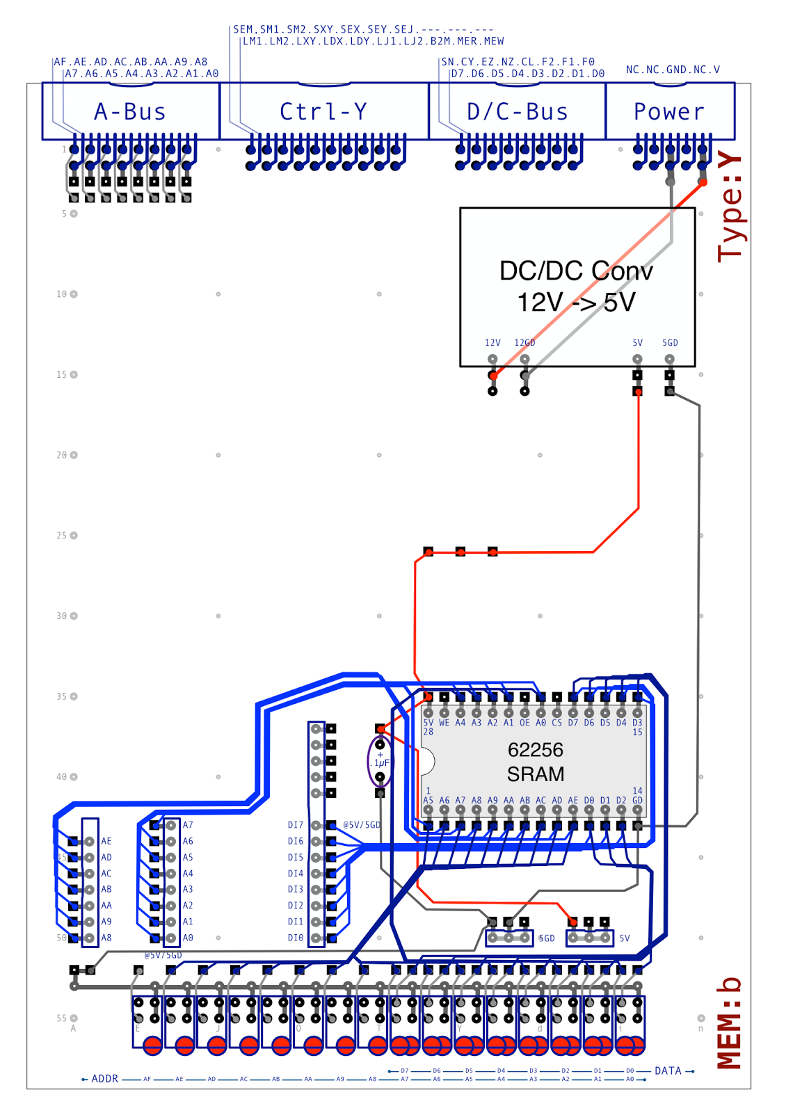
Finally, let’s add the remaining control lines:
There’s a little more going on this time. Starting at the address bus connector at the top left of the card we pick up the most significant bit (AF) and take it down to a relay at the middle right of the card. Whilst AF is low the chip select (CS) line is held low which enables the chip … when the AF line is high the chip select line is held high which disables the chip. This ensures that the chip effectively gets out of the way when using the higher memory addresses. Likewise the output enable line is connected or disconnected accordingly effectively vetoing the other memory card pulling the OE line low which would enable the output.
So that’s it for this card. I’ll continue the design in my next post where I’ll need to take all of those board interconnects and handle the differences in voltage between this card and the rest of the computer and wire out those inverted data bus outputs.