The design of the computer’s memory, incrementer and program counter are now complete but there’s one last piece of the ‘puzzle’ required to get the computer running a program. The controller now needs updating to orchestrate the ‘fetch and increment’ cycle. This cycle retrieves the next instruction from memory (into the instruction register) and then increments the program counter to point at the next instruction in memory. In this post I’ll cover the changes needed to the controller cards to implement this cycle.
The fetch/increment cycle consists of the following steps:
- Select Program Counter on to Address Bus and whilst
keeping selected:
- Read Memory on to Data Bus and whilst keeping
read:
- Load Instruction Register
- Load Increment Register (from incremented address bus value)
- Read Memory on to Data Bus and whilst keeping
read:
- Select Increment Register and whilst keeping selected:
- Load Program Counter
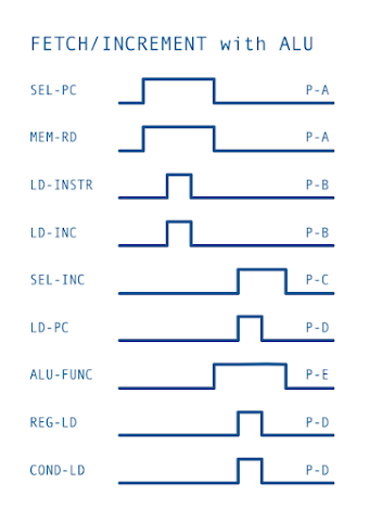
Visualising these steps as a timing diagram we get the following:
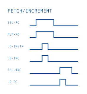
As with the ALU, SETAB and MOV-8 instruction classes implemented so far we need to make sure any value selected on to a bus is stable before using it. You can see this above where the SEL-PC and MEM-RD control lines are held on around the LD-INSTR and LD-INC calls to ensure the values being read stabilise on the address and data busses and aren’t dropped whilst loading the incrementer or instruction registers. In a similar vein we need to ensure that consecutive values placed on to a bus have a gap between them so that they don’t interfere with one another. You can see this effect between the SEL-PC and SEL-INC actions above.
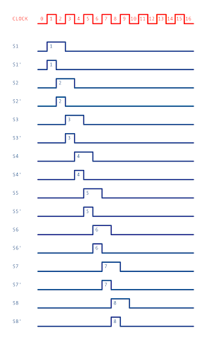
To implement these timing actions we need to revisit the sequencer and derived pulses. As a reminder, here is the timing diagram for the sequencer as it currently stands:
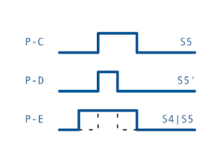
The ALU, SETAB and MOV-8 instructions all start operating from S4 onwards using derived pulses C, D and E as follows:
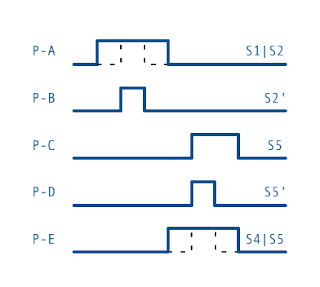
Similarly to get the instruction timings we need for the fetch and increment cycles we can derive additional pulses A and B as follows:
Effectively we’re using pulses C, D and E to run the loaded instruction at the same time as the program counter is moved on to the next instruction. This is fine as long as the loaded instruction doesn’t need to use the address bus. Any instructions that do need the address bus would have to wait a bit for the increment to be completed before performing their action. As an example, this is what the timing would look like for an ALU instruction loaded from memory:
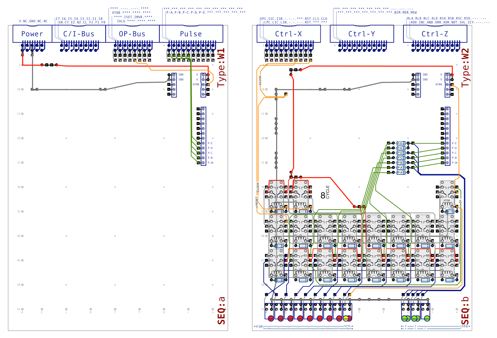
OK, so we know what we want to achieve so it’s time to update the sequencer and control card designs. Starting with the sequencer the design currently looks like this:
We have all the states we need in the existing 8 cycle finite state machine so adding pulses A and B is simply a case of pulling off the appropriate states and routing them out through the upper card as follows:
This gives us the derived pulses we’ll need so it’s on to the control card. We can implement the fetch/increment cycle with just four relays as follows:
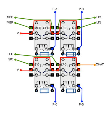
Each relay reacts to the four derived pulses P-A thru P-D and activates the corresponding control lines as appropriate. The program counter is selected and the memory read (SPC and MER) and then the instruction register and incrementer are loaded (LIN and LIC). Once that’s done the incrementer is selected (SIC) and then the program counter is loaded (LPC). The only extra item here that might need a bit of explanation is the ‘CHAT’ line which is used by other parts of the control card to know when is a good time to set the abort relay for the length of instruction … all instructions are 8 cycle for now so when CHAT is activated then the Abort-8 line will be set. Previously this was just hard wired to Pulse D.
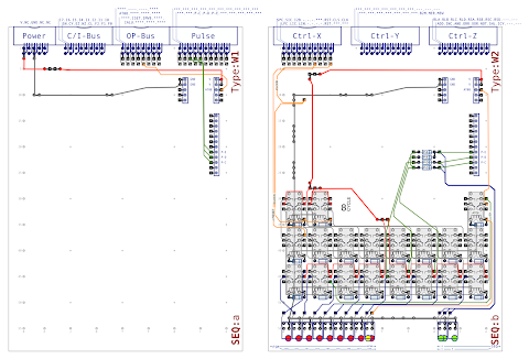
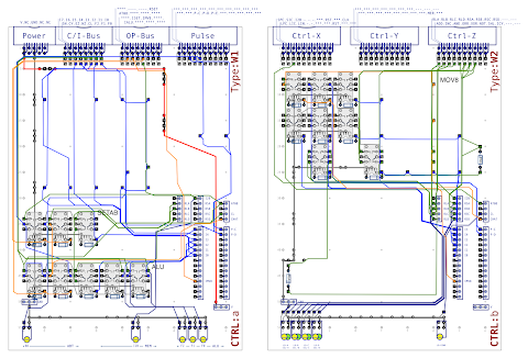
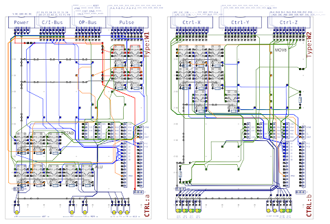
The fetch/increment relays are ready to go … they just need fitting within the control cards. Here is the controller design as it currently stands:
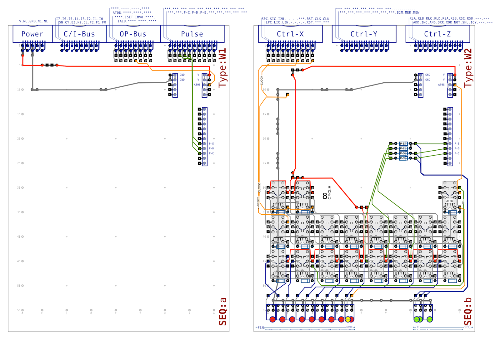
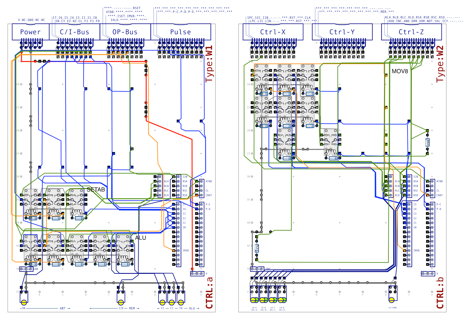
… and here’s how the design looks after adding the fetch/increment relays …
The four new relays are added in the top right of the upper control card (CTRL:a) and pick up the passing P-C and P-D lines alongside the new P-A and P-B lines. The CHAT output is routed through the SETAB and ALU blocks and down to the lower card to the MOV8 block. The control outputs from the four relays (SPC/LPC, SIC/LIC, LIN and MER) are routed through to the appropriate bus connector and status LED (via the lower card where necessary). As with the previous design of the controller you can see some of the lines take odd routes around the cards and this is where future parts of the cards will utilise those passing lines.
As always, if you’d like to see a larger version of these designs you can find PDF versions of the sequencer here and controller here.
That’s it … all the designs
are in place to be able to load a program in to the computer’s memory and then
have the computer execute that program line-by-line with no further assistance
from the user. In the next series of posts I’ll cover constructing these
latest cards and then giving the whole thing a whirl (at which point I’ll
likely do an updated ‘overview’ video on YouTube).