In my last post I covered the design of the 16-bit half adder which takes whatever value is currently on the address bus and increments it by one. To make this incremented value useable we need to create a register so that we can store the value ready for pushing back on to the address bus. Typically this incremented value would then be loaded into the program counter to get it ready for the next instruction in memory.
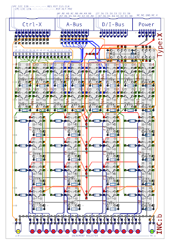
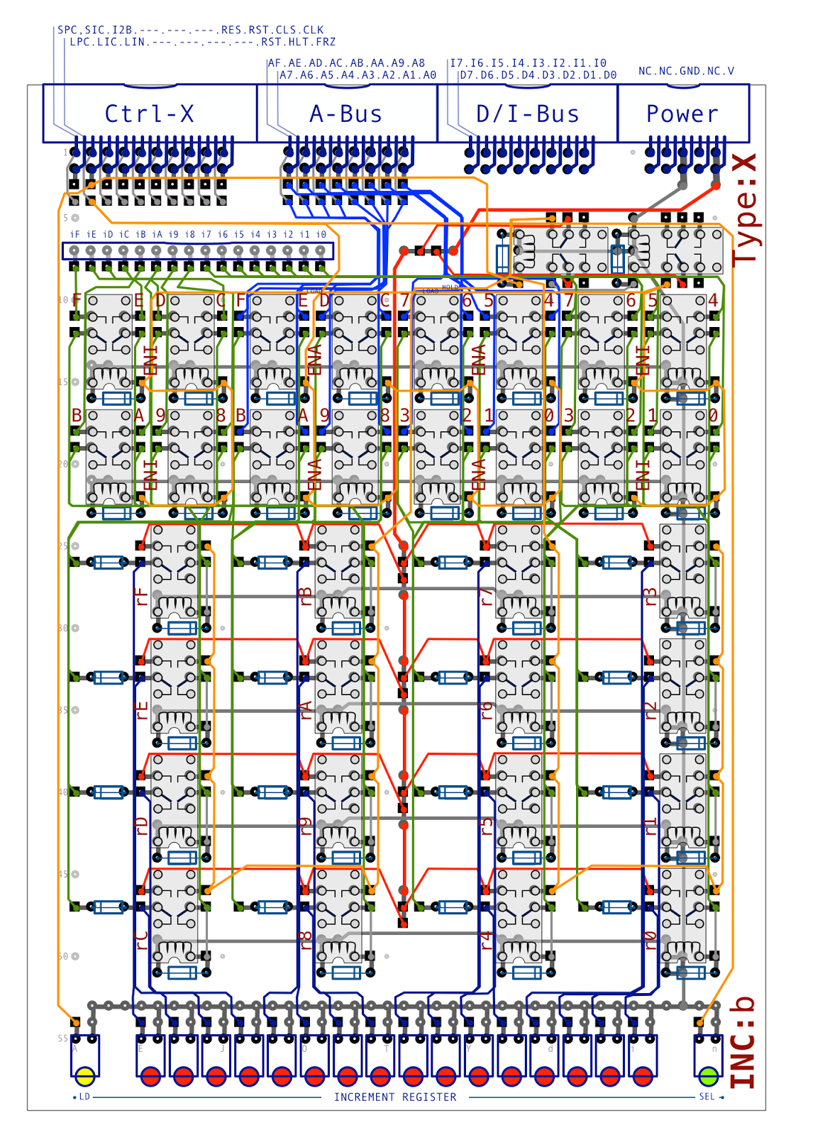
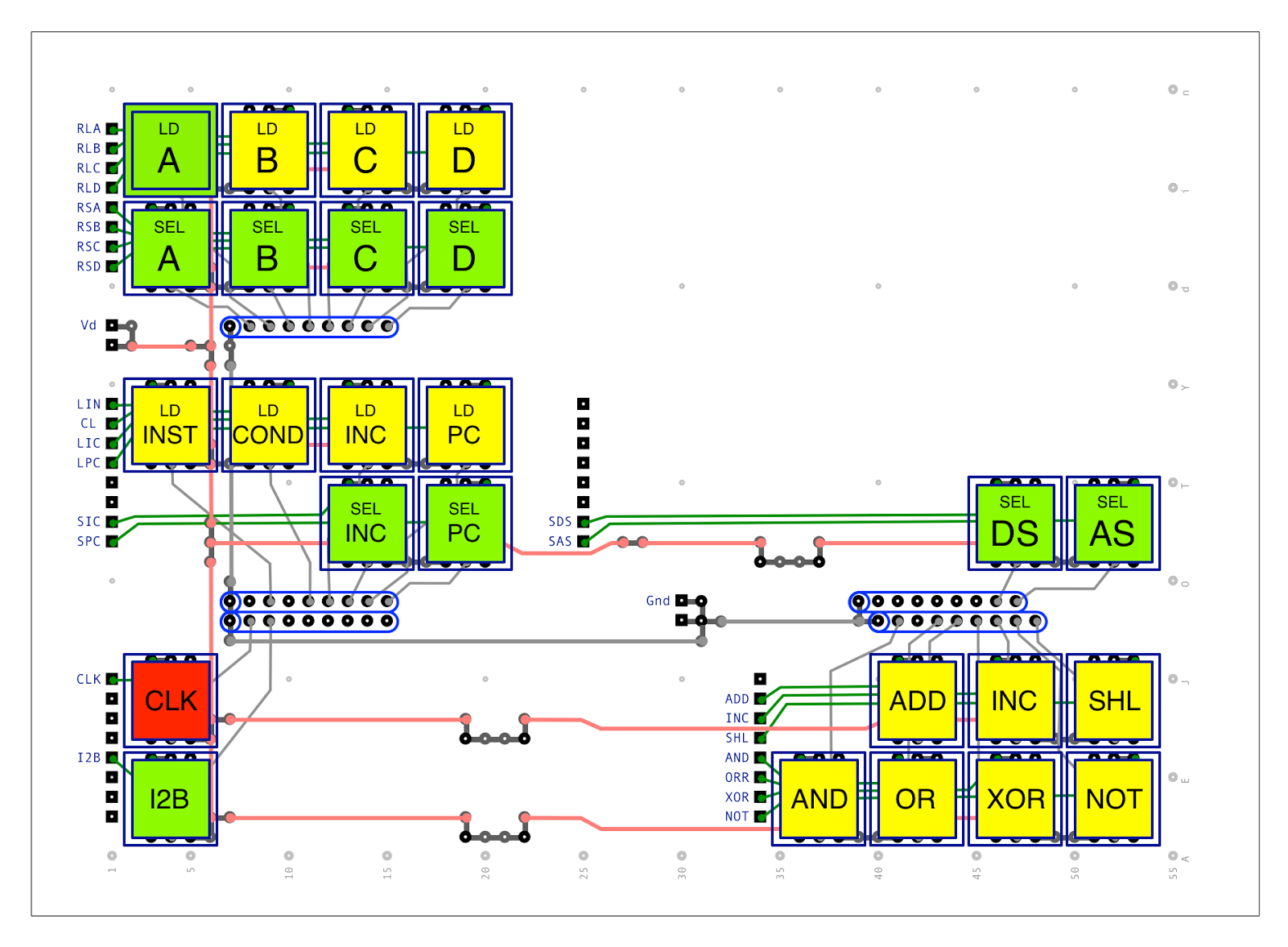
By now you’re probably sick of seeing register designs (I know I am) and this particular register is similar to all the other registers seen so far in the computer. Just like the program counter this register holds a single 16-bit value which can be gated on to the address bus. The main difference here is that the register is loaded directly from the 16-bit half adder via an inter-card connector. Here’s the design for this register:
As with other register cards the relays that latch each bit value are on the bottom half of the card with bit 0 at the bottom right and then with bit relays running up in columns and towards the left of the card with bit 15 at the top left. As usual there’s a diode on the output of each bit to ensure that when the register is connected to the address bus there’s no back-feed that could corrupt the register if another card was gating to the address bus at the same time.
In the upper half of the card you can see the gating relays. These are arranged in groups of four relays forming a square, that is, if you look at the left there are two relays laid out vertically with another two relays to the right of those … this forms a single group. Going from the right to left the first group gates the incremented value (from the half adder) for bits 0 thru 7 … next group gates bits 0 thru 7 to the address bus … next group gates bits 8 thru 15 to the address bus … finally, at the left of the card, the last group gates bits 8 thru 15 from the incremented value.
So with the designs of the 16-bit half adder and 16-bit incrementer register ready to go we can bring the two cards together to form the final incrementer design:
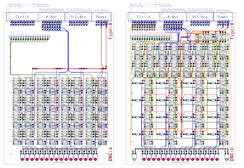
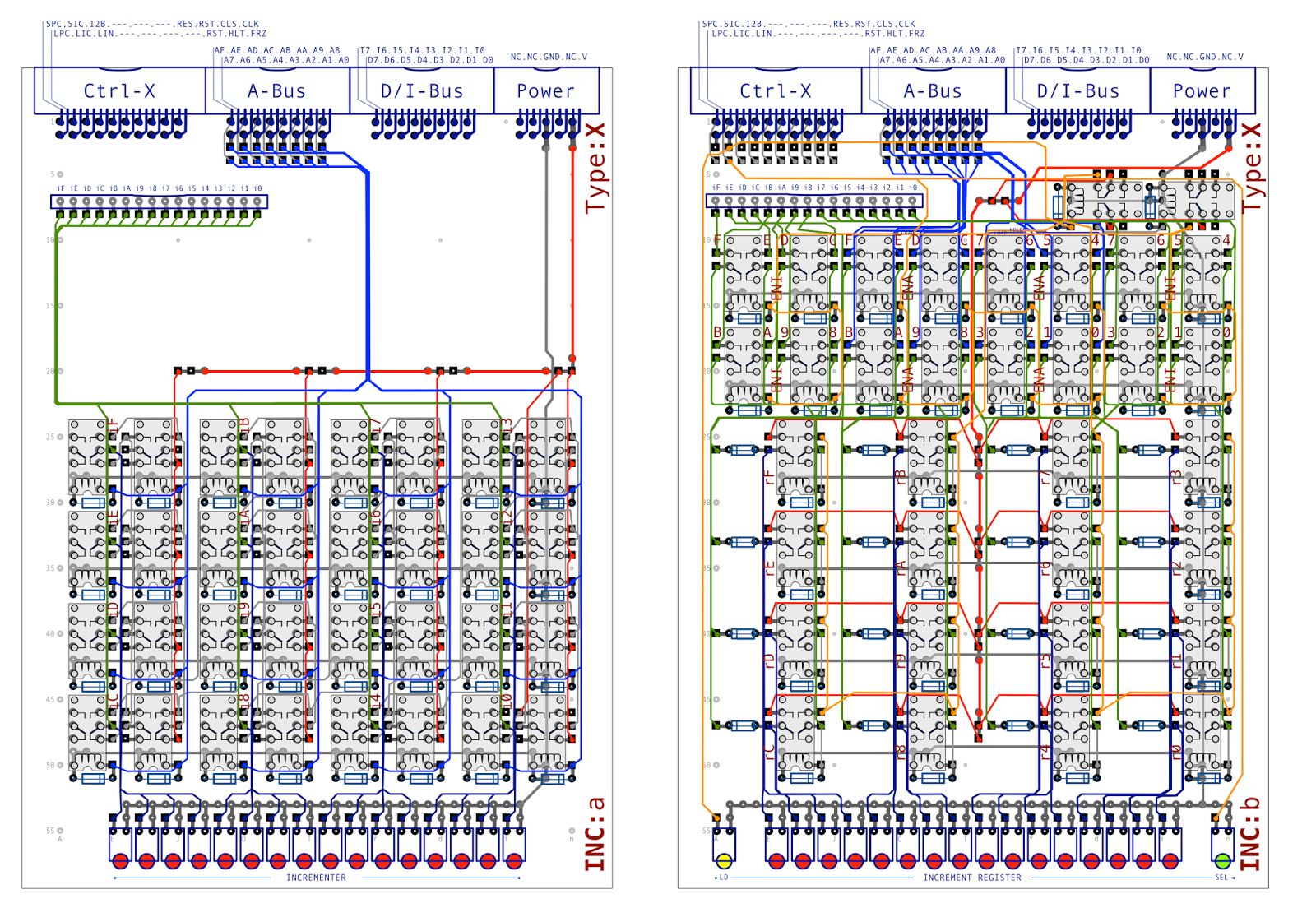
As usual if you’d like to get an extreme close up of the above you’ll find the incrementer design available here in PDF format.
With the incrementer design done all that remains is to update Display A adding two extra buttons … one to load the incrementer register from the half adder (LD INC) and one to select the incrementer register on to the address bus (SEL INC). With the added buttons Display A now looks like this:

Again, you can find a PDF version of this design here and another version without the buttons.
Finally, to wrap things up, I’ve updated my relay computer simulator that now looks like this:
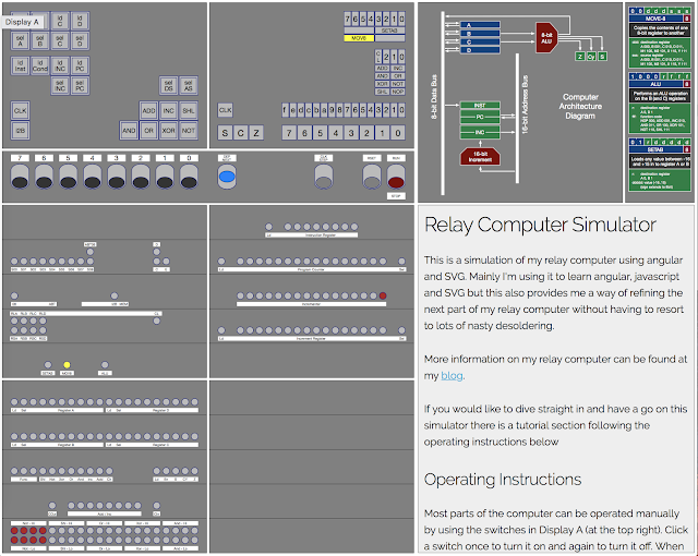
The latest version of this can be found here (although note that I only ever host the latest version so as this post gets older the simulator might be newer than you’d expect). Feel free to fire this up and have a play with the program counter. If you’re interested in what’s behind the simulator you can see all the source code on my GitHub page.
So, with the recent round of designs we can now store where in memory the current instruction is stored (with the program counter) and then increment that ‘pointer’ to the next location in memory. What’s missing? … well, the memory itself of course … and that’s what I’ll cover in my next post.