Typical isn’t it?! … you wait 10 months for a post and then two come along at once. Well, all being well, this should be the first of a short flurry of posts as I move on to the design of the incrementer.
The incrementer takes any value currently on the 16-bit address bus and adds one to it, or rather, it increments it (clue is in the name of course). Typically that value on the address bus is going to come from the program counter (in order to point it at the next instruction in memory) but it’ll also be possible to bump the upcoming XY register eventually too.
One complication in the incrementer is that because the address bus can only hold one value at a time it’s necessary to have a built-in 16-bit register which can hold the result of the incrementation ready to be gated back on the address bus and off into the destination register. So, for example, the PC register is selected and the incrementer register loaded with the PC value +1. Once that’s done the incrementer register can be selected and the PC loaded with the new value.
Effectively then the incrementer consists of two halves … the 16-bit increment register and a 16-bit half adder that feeds it. Half adder? Well that’s the part I’ll cover first by taking a look back at the half adder’s bigger sibling, the full adder, which appeared in the design of the ALU arithmetic card. Here’s the 1-bit full adder relay wiring diagram again:
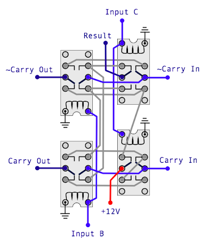
This takes two 1-bit inputs (B and C) and adds them together to produce a 1-bit result. Any carry (when B and C are both set) is passed on to the next adder circuit and likewise any carry coming in from a prior adder circuit is taken in to consideration. Effectively the circuit implements the following ’truth table':
| Carry In | Input B | Input C | Carry Out | Result | |
|---|---|---|---|---|---|
| 0 | 0 | 0 | 0 | 0 | |
| 0 | 0 | 1 | 0 | 1 | |
| 0 | 1 | 0 | 0 | 1 | |
| 0 | 1 | 1 | 1 | 0 | |
| 1 | 0 | 0 | 0 | 1 | |
| 1 | 0 | 1 | 1 | 0 | |
| 1 | 1 | 0 | 1 | 0 | |
| 1 | 1 | 1 | 1 | 1 |
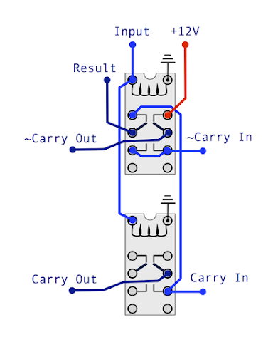
As you may have guessed a half adder only needs to deal with one input rather than two and has the following truth table:
| Carry In | Input | Carry Out | Result | |
|---|---|---|---|---|
| 0 | 0 | 0 | 0 | |
| 0 | 1 | 0 | 1 | |
| 1 | 0 | 0 | 1 | |
| 1 | 1 | 1 | 0 |
Likewise this simplifies the relay wiring diagram to the following:
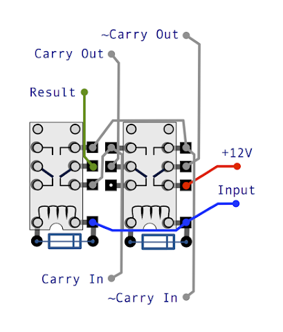
This layout focusses on lining up the carry in and outs so that each unit can be stacked horizontally alongside the next one. To fit the full 16 half adders on the card I’m going to take this design and rotate it 90 degrees so I can stack the units vertically. Doing that, and using the schematic style used for other cards in this computer, we have the following:
… and that’s all there is to a 1-bit half adder. In the next post I’ll cover linking 16 of these units together to make the full 16-bit half adder.