Well, the good news is I’ve just passed a major milestone in constructing this relay computer … it can now perform a single instruction in full firing the various control lines as needed. The bad news … I’m rather behind in blogging about it so this will be the first of a couple of ‘catch up’ posts which will culminate in a video showing off the computer as it currently stands.
The last outstanding item from the MOV-8, ALU and SETAB series of construction is updating the computer’s user interface so that the contents of the instruction register and the actions of the control and sequencer cards can be observed. The first job was to apply the legends to the new buttons and indicators that I’d be adding to the two display cards. Here’s a close up picture:
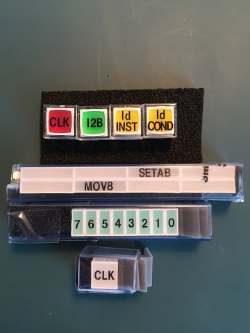
The buttons at the top are (from left to right) clock, instruction to bus (I2B), instruction load and condition load. Below that are the instruction class indicators: MOV8 and SETAB. The ALU instruction class isn’t indicated as the specific ALU operation is shown in the ALU indicator group. Next is the instruction opcode byte and finally the clock indicator.
With the additional buttons installed on Display A we get the following:
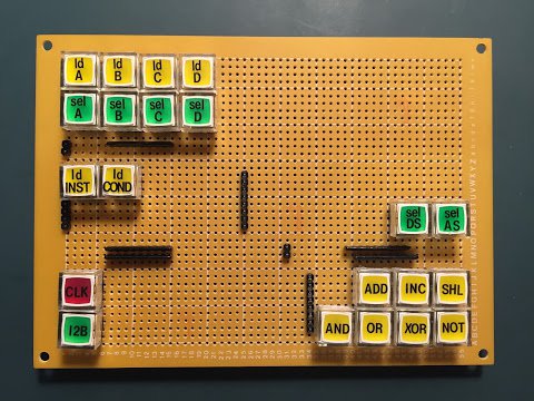
Previously on this card the Address Switch Select (sel AS) was wired up to the Load Condition register line but now it has its own dedicated button (ld COND) I’ve removed the temporary wire link.
Adding the new indicators to Display B we get the following:
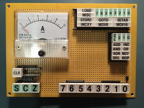
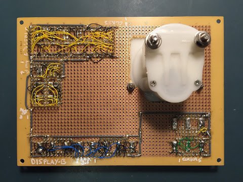
The instruction register op code is shown at the top right and around that is the decoded instruction class that op code represents (excluding ALU which is shown separately in the block below). I decided to add the labelling for all the other instruction classes that the computer will eventually support as I didn’t want to risk damaging the indicators when I’d later have to remove them to add the additional legends. Similarly on the rear of the card I’ve soldered up all of the instruction class indicators to save things getting messy later on. Lastly on this card the clock indicator sits above the three condition registers.
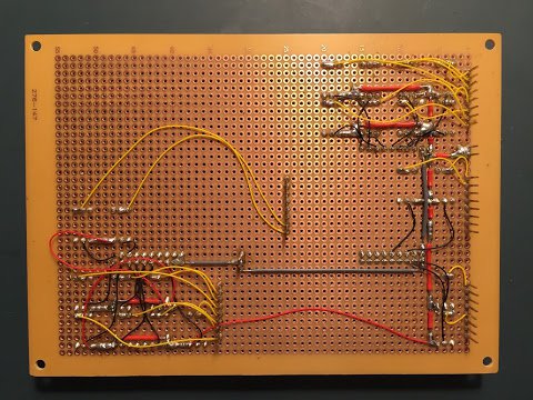
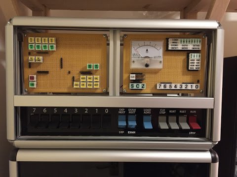
With both display cards installed back in the upper enclosure it looks like this:
With the display cards updated the next job was to hook up the right hand primary switches as I’ll need the clock step and reset (RSET) switches to help operate the computer when everything constructed so far is tested together. The switches are soldered up to some ribbon cable much the same way the left hand primary switches were:
The upper enclosure as a whole then looks like this:
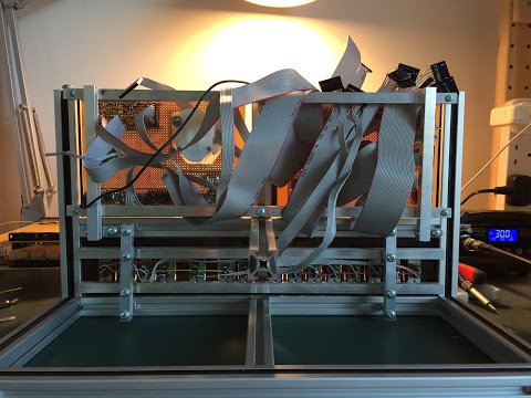
There’s quite a lot of ribbon cables coming off the display cards now and these all need wiring out on the display distribution card:
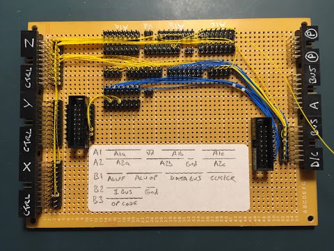
There’s quite a bit added to this card. Firstly, the instruction op code is brought in on the new 16 pin straight IDC socket on the right. This is the C/I bus (control and instruction) and sits next to the D/C bus (data and control) on the far right. The other 16 pin straight IDC socket on the left is the OP bus which brings in the current decoded instruction class. This sits to the right of the X and Y control busses. Both these new sockets are wired out to the display cards as appropriate.
To aid wiring out I’ve added a sticky label and written on which display cables go where and I’ve also written on the edge connectors in white pen. The yellow ‘flying’ lead seen heading off the photo to the right connects to the auxiliary control card for activating the Select Data Switches operation (sel DS). Speaking of which … here is the updated auxiliary control card:
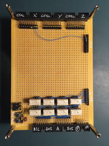
Not too much has changed here … the right hand primary switches are wired out to the X control bus and then I’ve marked up the connectors in white pen again.
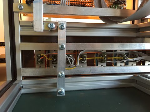
That’s it for now on the upper enclosure … the computer is getting very close to the point where I’ll be able to test all the cards constructed so far together. One missing piece is the backplane that the new ‘W’ cards will sit on. Unfortunately this one won’t be straightforward as the ‘W’ backplane has W1 and W2 style connectors which will make wiring up the backplane challenging - anyho, I’ll leave that for my next post.