I’m just about at the half way mark now for getting the computer to operate the MOV8, ALU and SETAB instructions. The easier cards are out of the way now … time for the slightly more complex ones. In this post it’s the sequencer cards which will deal with the ‘when’ of instructions by sending out timing pulses which the upcoming control cards will then use to operate the various control lines of the computer at the right time.
Note there that I did say sequencer ‘cards’ and not ‘card’ because there’s two of them this time. This is the first part of the computer that will be constructed across two cards stacked together rather than all on a single card (the upcoming control unit will also be spread across two cards). This is for two reasons: firstly the sequencer needs access to more connections than a ‘regular’ card but secondly there’ll be so much to fit in that it physically wouldn’t fit on one card.
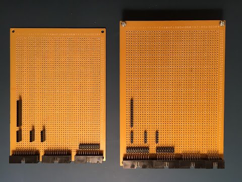
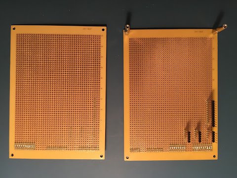
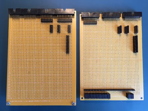
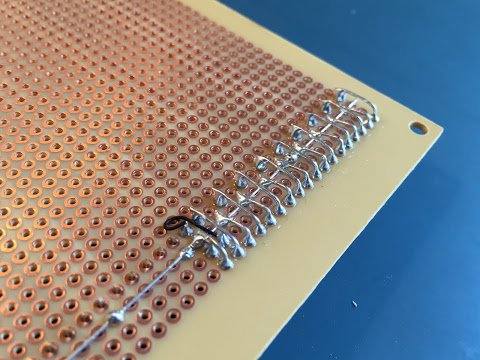
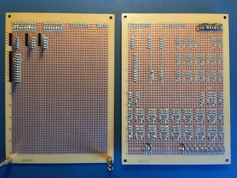
Working across two cards does present additional challenges in the construction … mainly around how to get the required signals that are private to the sequencer between the two cards. I considered many options but in the end a system of stacking header pins seemed the best route forward. So, to start construction I soldered down the ribbon cable connectors and board interconnects … once done it looked like this:
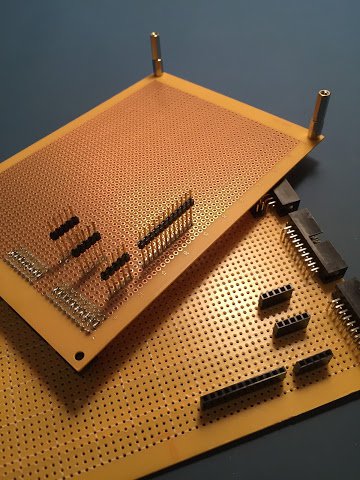
To keep the two cards stable I also added some PCB stand-offs in the front corners. Thankfully the distance between cards in the enclosure can be made up using standard stand-off lengths. I’d like to say I planned it that way but of course I didn’t … it’s just another one of those happy coincidences which happens when everything is on a 0.1 inch grid.
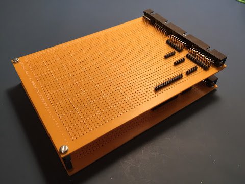
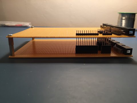
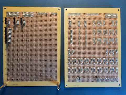
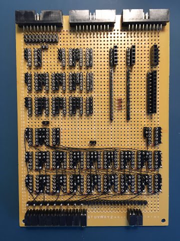
To stack the cards the upper card header pins are aligned and inserted into the respective sockets on the lower card producing a unit that looks like this:
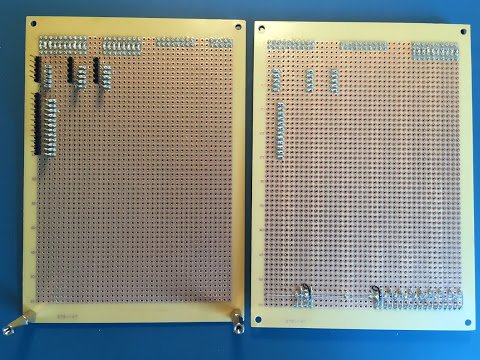
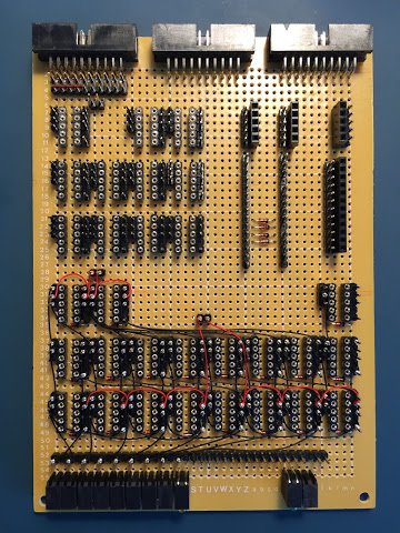
With the basic connections in I moved on to soldering in the wire wrapping posts for the interconnects and LEDs along with the LEDs themselves.
One problem with the board interconnects on the upper card is that it does make soldering a little fiddly as you have something protruding up from the board getting in the way … plus that ‘something’ will melt (or at least the plastic parts of it will) if you apply a soldering iron to it.
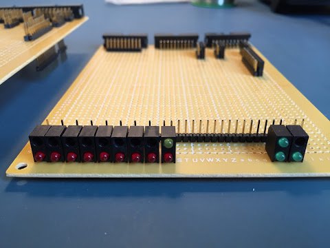
For the LEDs I’ve continued using the newer method of soldering the LED cathodes together with bits of trimmed off diode/LED legs as it makes soldering much easier. This is the first time, however, that I’ve tried this technique on double height LED holders. Generally the concept stays the same … join all the cathodes together … but for the holders that have LEDs in their upper slot I need to add a small Kynar wire link to get that LEDs anode to the wire wrap post. It’s all a bit fiddly but as long as you have patience and a steady hand it usually comes off OK.
Next up were the relay sockets and associated wire wrap posts:
I’ve actually soldered down the relay sockets for the upcoming 10 and 12-cycle relays on the lower card in addition to the required 8-cycle relay sockets. This is because soldering these sockets down is a really fiddly job and I know that when I come back to this card to add functionality later it’ll be a real pain when there’s relays and all the wiring getting in the way. I’ll not bother soldering the underside of these sockets much further but at least the fiddly upper side is done. I’ve not done anything on the upper card although eventually this will hold further cycle relays all the way up to the full 24-cycle sequencer.
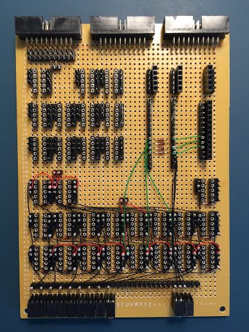
Next job was to solder in the flyback and feedback diodes (which ensure produced outputs don’t feed back into parts of the sequencer’s finite state machine):
The final soldering job was to put in the power and ground lines:
This time around I finally got bored of cutting and stripping all those short bits of coated wire for the ground lines and decided to give the same technique I use for grounding the LEDs a try for the relays. This does mean that all the grounds are exposed for their full lengths but on the plus side it was much quicker and easier to put everything together. I’ll see how I feel about it but I’ll more than likely do the same on the next card.
There’s some temporary Kynar wires in the power and ground lines and these are just to ‘hop’ over future parts of the card where the lines will eventually go through. The Kynar wire, of course, can’t handle all that much current but it should be fine for now.
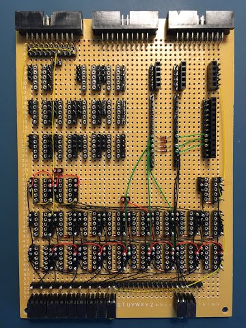
With the soldering done it’s on with the wire wrapping. The sequencer probably has the most complicated wiring yet (second only, maybe, to the ALU arithmetic unit).
With the wire wrap done the relays can then be placed in their sockets:
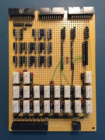
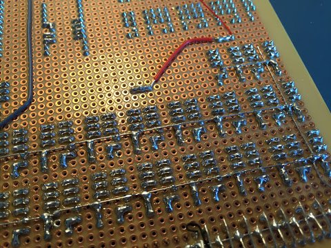
This is almost the last step however to make the sequencer useable up to the 8th cycle I need to add a couple of extra temporary Kynar links that will connect stages 7 and 8 back to stage 1 and 0. Later on when longer cycles are implemented stage 9 and 10 will provide the required lines to keep stages 7 and 8 alive … for now, in their absence, the first stages will do the same job. With the temporary links in place the lower card looks like this:
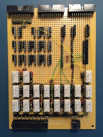
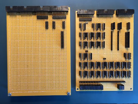
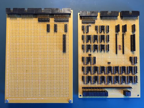
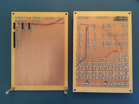
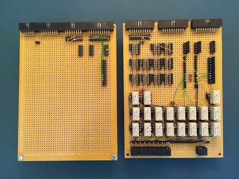
So, finally, that’s the sequencer complete for 8-cycle instructions. The card will be extended over time as longer cycle instructions are introduced but for now the sequencer as a whole looks like this:

As usual I’ve put a video together that demonstrates the sequencer in operation. In this video I give a quick overview of the cards and then demonstrate running through the 8 stages of the finite state machine and producing the three derived pulses C, D and E.
That’s it for the sequencer … at least for now. It produces all the pulses that will be needed for the computer to perform copying values between registers, loading values from the opcode and performing ALU operations. The final step in making these operations a reality is to construct the control unit … again though, just enough to operate these three 8-cycle instructions. The control unit is similar to the sequencer in that it will also be spread over two cards although fortunately it’s wiring will be quite a lot simpler as most of it is just combinatorial logic.