Over my last seven posts I’ve been slowly putting together the card designs so that the computer will be able to operate the MOV-8, ALU and SETAB instructions. The final step in this series is to update the designs for the two display cards along with the main switches to work with the new cards added recently.
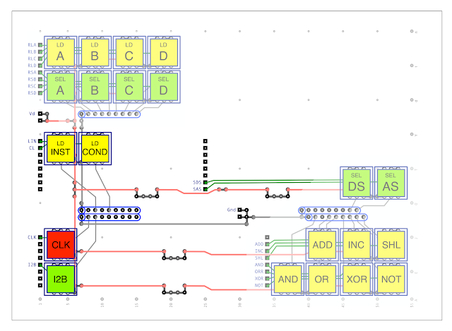
Diving straight in here is the latest version of the Display A design:
This is the card that sits in the upper left of the enclosure and doubles up as a display as well as a means of directly operating some of the control lines. Each block on the diagram is an illuminated tactile switch that directly displays and operates an individual control line. I’ve faded out all of the existing switches so that the new ones are highlighted.
The two new yellow switches in the middle drive the Load Instruction Register and Load Condition Register lines. Previously I’d temporarily wired up the ‘Sel AS’ switch up to the load condition register line but now it’ll have its own dedicated switch and the ‘Sel AS’ will be used later on to load the address bus with a value from the front switches.
At the bottom left of the card is the new red ‘CLK’ and green ‘I2B’ switches. The ‘CLK’ switch directly operates the clock line so repeated pressing of this will drive the sequencer when activated. The I2B drives the Immediate To Bus line that gates a value held on the instruction bus over to the data bus. This is usually operated during the SETAB instruction but can be operated directly from this switch for testing/debugging purposes.
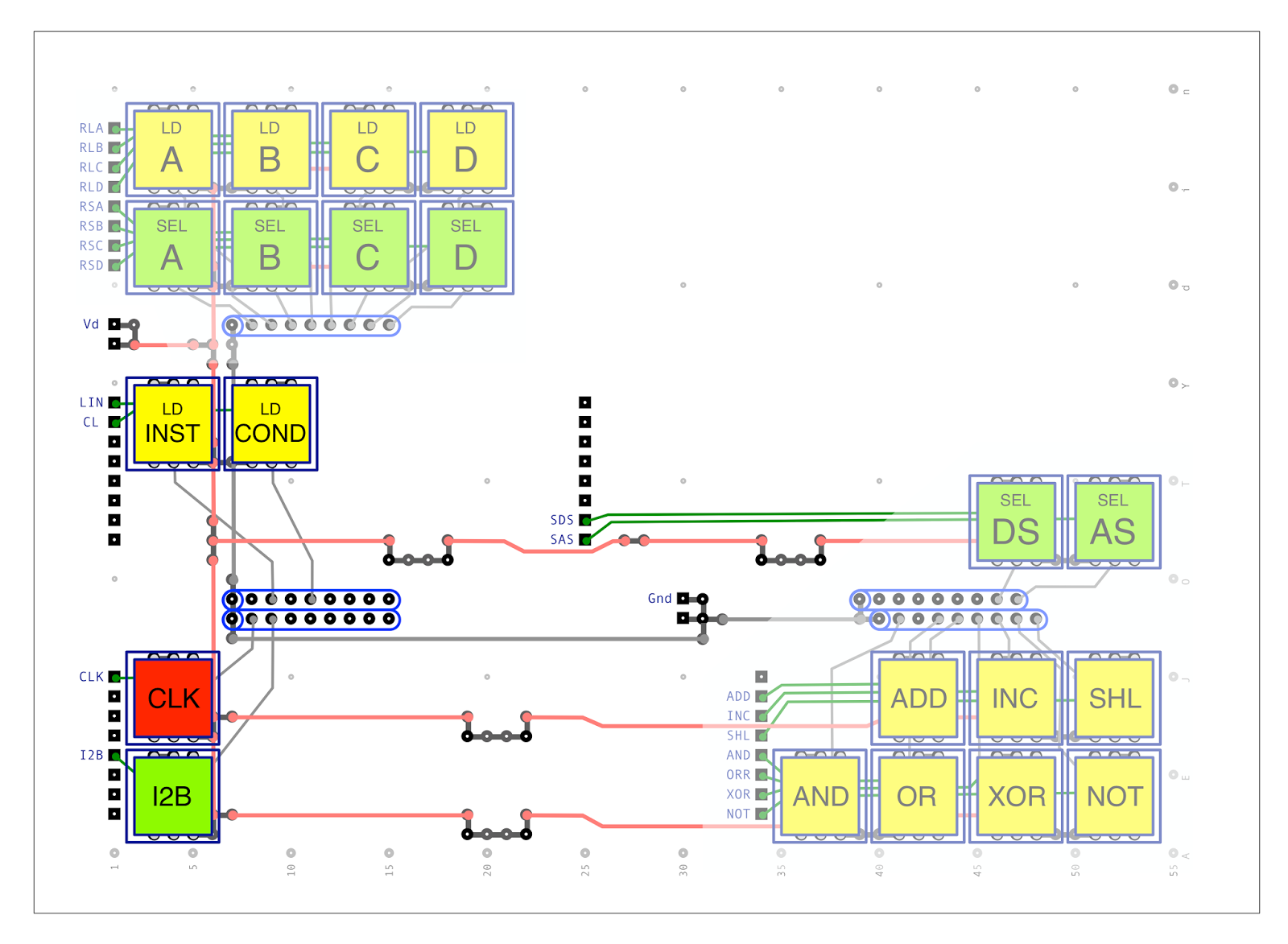
The second display card (Display B) sits in the upper right of the enclosure and will now look like this:

All the blocks on this card only display a value and are not interactive like the blocks on display A. At the lower left of the card is the new ‘CLK’ display which repeats the clock line value also shown on display A.
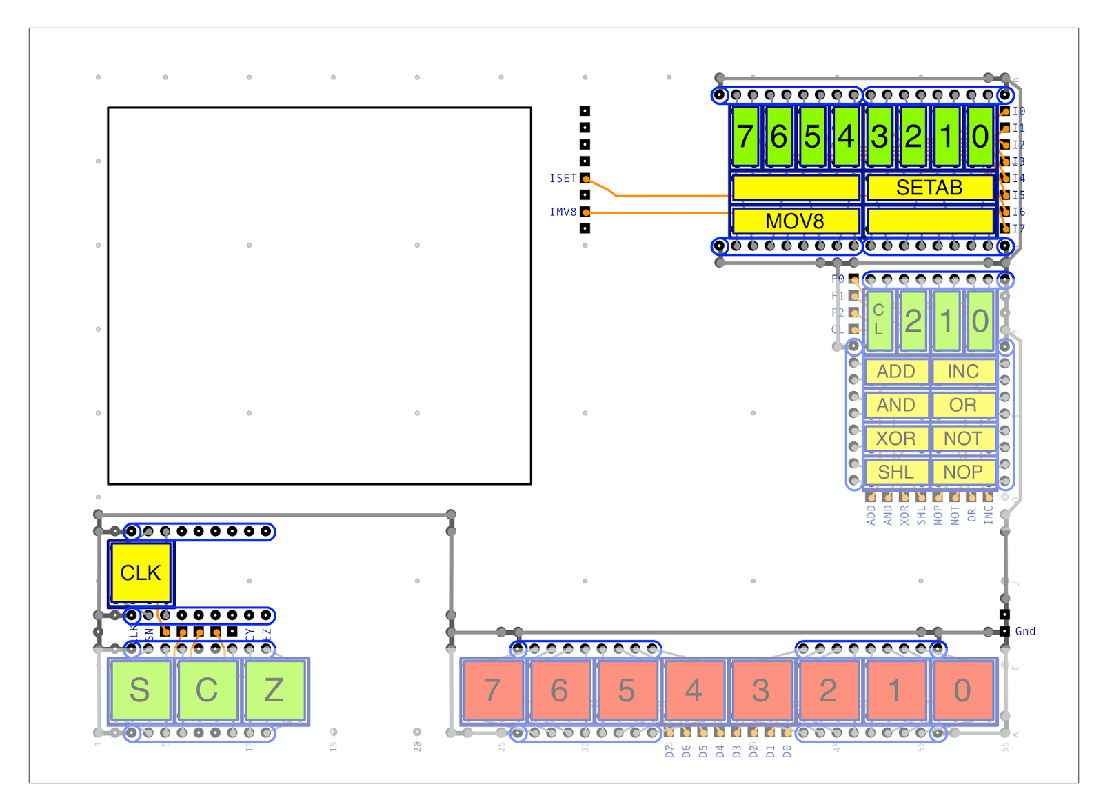
The main addition to Display A is at the top right which shows the current 8-bit instruction bus/register value and below that the derived instruction class. Only SETAB and MOV-8 instruction classes are shown as any ALU operation will show up on the ALU display just below.
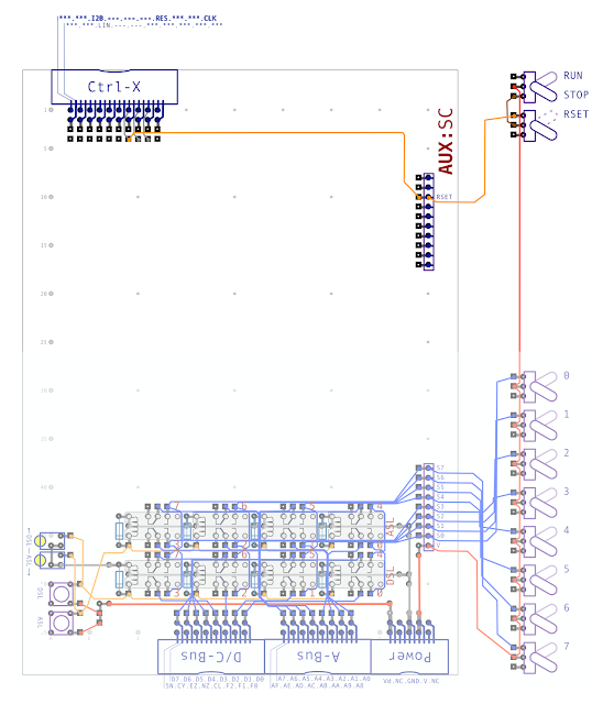
Finally there’s a small addition to do on the front panel switch control card:
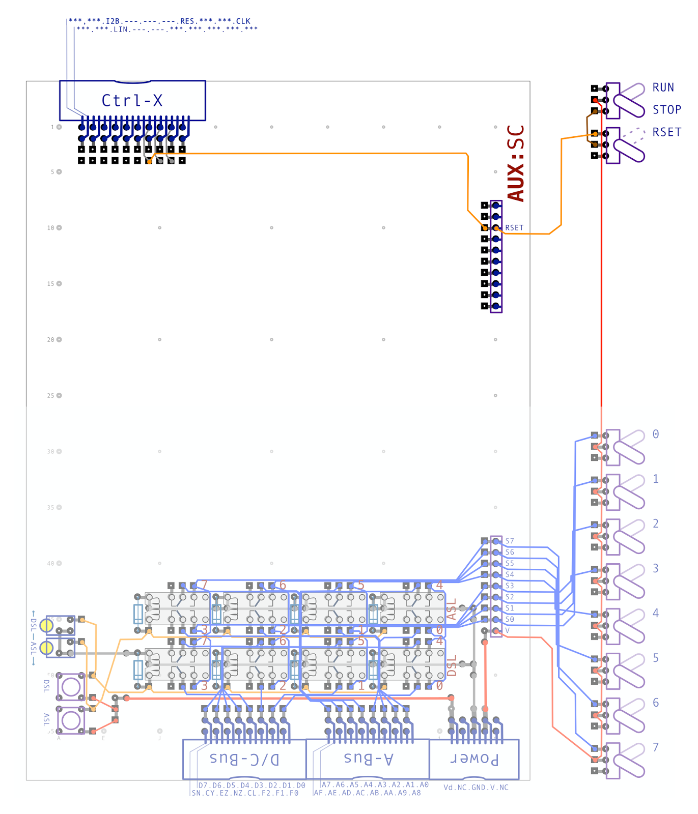
The lower half of the card shows the existing gating relays which pass the 8-bit value set on the front switches to either the data or lower 8-bits of the address bus. The small addition is at the top of the card where the reset switch is hooked up to the Ctrl-X bus so that the sequencer can be reset when needed. Of particular note here is that the reset switch is only powered when the start/stop switch is in the ‘stop’ position. This ensures that when the computer is running the user can’t accidentally interfere with the computer.
Updated PDF versions of the above designs are as follows:
- Display A
- Design with key caps shown
- Design without key caps (showing internal LED wiring)
- Display B
- Design with indicator faces
- Design without indicator faces (showing internal LED wiring)
- Aux Switch Control
… and that’s it … all the designs are in place so finally I can get the soldering iron out and start doing some construction. I’ll work in pretty much the same order I did the designs so it’ll be the instruction register first followed by the decoder. Both these are fairly straightforward cards so these should come together quite quickly and then it’ll be on to the more involved sequencer and control cards. Just before I do get stuck in to the construction though I’ll probably do a very quick post showing the terrible things I’ve done to a set of IKEA Ivar shelves to make my new workbench.