So far I’ve got the design complete for the instruction register along with the initial design for the decoder and so I’m well on the way to having the computer perform MOV-8, ALU and SETAB instructions. Later I’ll get on to the control card design where the computer will operate the control lines according to the 8-bit opcode stored in the instruction register. Before that though there’s the sequencer card which will generate the pulses that drive the control card.
There’s two halves to the sequencer card: the finite state machine (FSM) and the pulse distributor. I’ll cover pulse distribution in my next post as that is driven directly by the FSM. The FSM itself is driven by the clock signal which at the moment will be generated manually using the clock switch on the front of the computer but will eventually, of course, be generated automatically by the clock card.
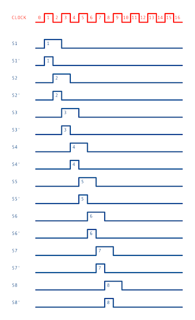
The FSM moves from state to state on each clock transition, that is, when the clock line goes high-to-low or low-to-high. Because the sequencer operates on each clock transition the operating speed of the computer is twice that of the clock … so if the clock cycles 3 times a second (3Hz) then the computer can perform up to 6 operations per second (6Hz). Each state produces a pulse Sx’ that lasts one clock ’tick’ and a pulse Sx that lasts two clock ’ticks’ (one clock cycle). Diagram wise the pulses look like this:
Eventually further states will be needed as more complex instruction classes are introduced but for now the MOV-8, ALU and SETAB instructions are all operable under an 8-cycle FSM.
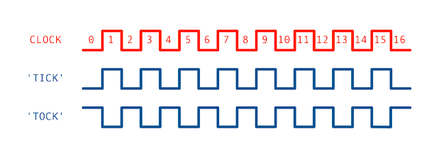
The first step in designing the sequencer’s FSM is to extract the ’ticks’ and ’tocks’ (like the noise an old pendulum clock makes) from the clock signal so that we obtain one pulse train that matches the clock and one that is the inverse of the clock as follows:
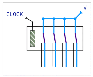
This is very straightforward with relays that contain SPDT switches as follows:
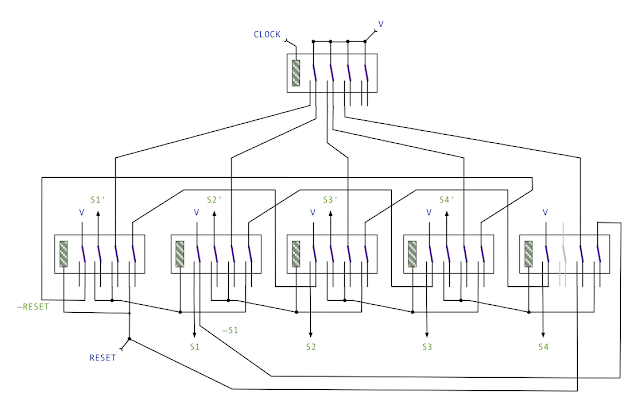
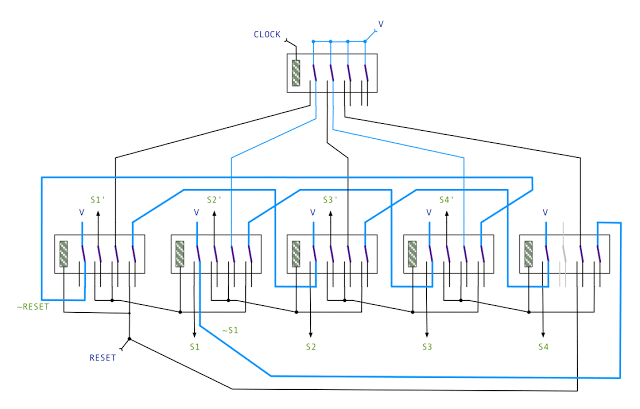
At its heart the sequencer FSM consists of a ‘ring counter’ which will move through each state upon a clock transition and then resets following the final step. There’s quite a bit of wiring in a ring counter so I’ll start with a simpler example … here’s the counter design for four stages:
To get the four stage FSM above going the first stage relay at the bottom left needs activating … this can be done by temporarily activating the RESET line. Once the first relay is activated it is held on by the feed it receives from the third stage relay.
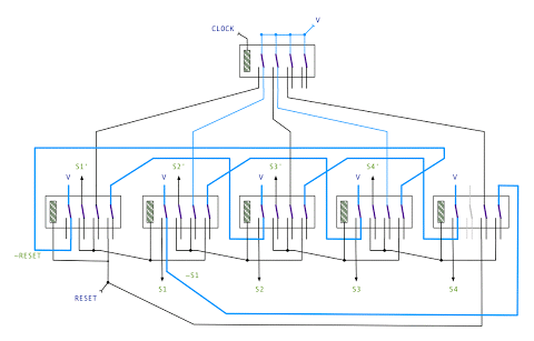
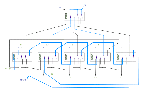
With the first relay activated and the state machine ready to go the clock can be started which will then activate the second relay then the third and then the fourth. When the third relay is activated the first drops out and when the fourth relay is activated the second relay drops out and so on. This pattern of operation continues until the final relay is reached.
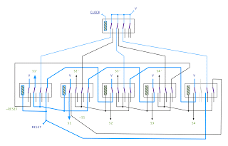
When the final relay is reached the RESET line is activated starting the cycle again.

Note that when the FSM is resetting the fourth relay channels the active clock line to the RESET line which then activates the first relay which then in turn activates the second relay which cuts the hold line on the fourth relay turning it off. The diagram above shows the state the FSM ends in following all this happening.
To make a FSM with more stages the pattern of relays and wiring is carried on as far as needed. To make things a bit easier to see I’ve put together the diagrams above into an animated gif below showing the four stage FSM in operation:
As mentioned above the FSM on the sequencer card will eventually have many more states so for the 8-cycle instructions we need a way of reseting the FSM early and the abort relays will make this happen when set. This simply activates the RESET line earlier when needed.
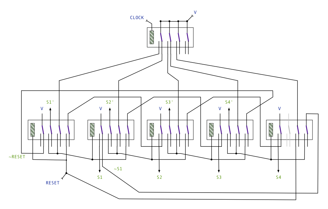
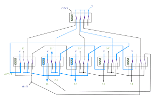
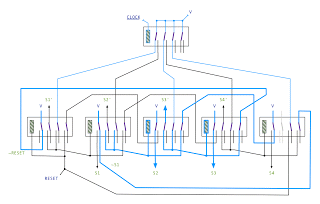
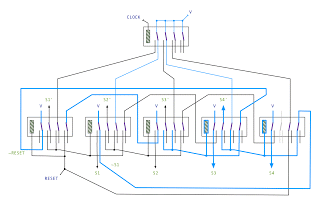
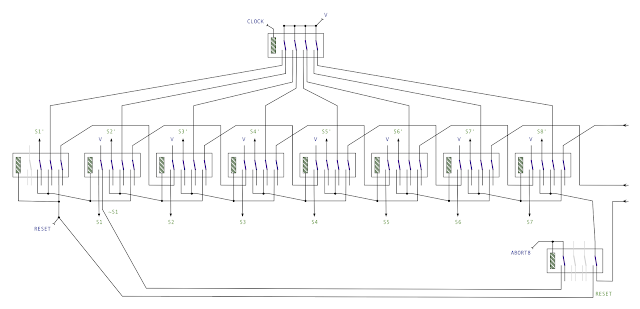
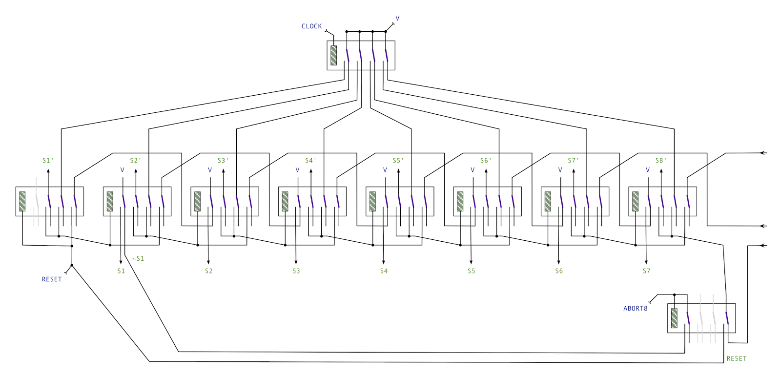
Building on the simple 4 stage FSM here is an 8 stage version that can continue on to further stages with ABORT8 line to end at stage 8:
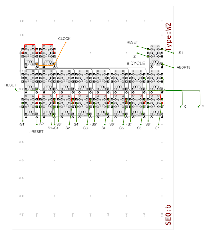
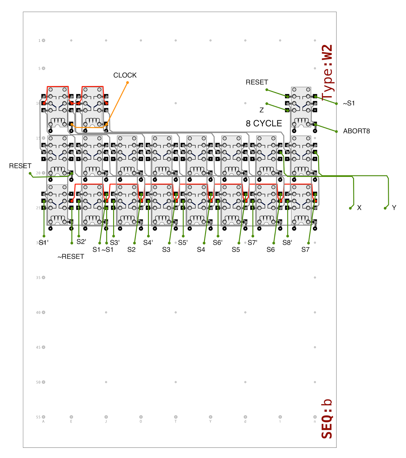
It is the 8 stage FSM above that I’ll be transferring now to the sequencer card design. As with all the other cards I’m using relays that have two SPDT switches and building on the usual 55 x 40 hole pad board. Here are the relays and internal wiring for the 8 stage FSM above:
As usual I’ll want the card to display the current state of the FSM so I can see what the card is up to. 8 red LEDs show states S1’ through to S8’ using the usual 12V LEDs with integral resistor. Note that only the Sx’ states are shown and not the longer Sx states effectively creating a single light that moves across the row of LEDs. Additionally there is a yellow LED above S8’ which shows when the ABORT8 signal is set thereby marking the point where the FSM will reset. Diagram wise it looks like this:
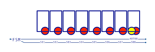
This pattern of LEDs will continue when extra stages are added to the FSM in future for the instructions that require longer cycles. Each block is made up of a bi-level LED holder with all the state LEDs on the bottom row and any abort LEDs on the top row.
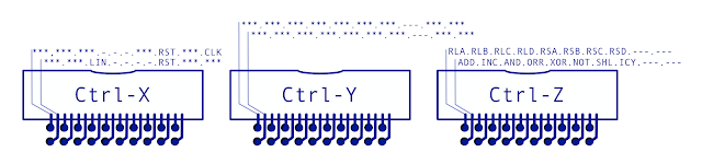
Next up is the connections to other parts of the computer. In my last post for the decoder design I introduced the new W1 and W2 connection types. The sequencer will eventually be spread across two cards (one of each type) so that it has access to all the busses it needs and has enough room for all the relays that will eventually be required … I’ll cover this more in my next post when I add the pulse distribution to the sequencer. For now all that is needed is the clock signal and that comes in on the Ctrl-X bus via the W2 connectors.
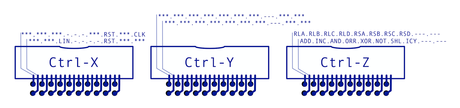
The ‘W2’ connections bring together the Ctrl-X, Ctrl-Y and Ctrl-Z busses that come in from the X, Y and Z type cards. The diagram of the connectors look like this:
This shows the three right angled boxed headers — from left to right these are: 10+10 Ctrl-X bus, 10+10 Ctrl-Y bus and 10+10 Ctrl-Z bus. Lines marked ‘***’ are lines that will be used by future ‘W2 type’ cards and the lines marked ‘—’ are unused/spare. Note that there’s no power connector on this board as that’ll be supplied by the W1 card which joins this card to make the full sequencer. The lines on each connector are as follows:
- Ctrl-X Bus (type X control bus)
- LIN … Load Instruction Register
- RST … Clock Reset
- CLK … Clock Signal
- Ctrl-Y Bus (type Y control bus)
- Ctrl-Z Bus (type Z control bus)
- RLA/B/C/D … Register Load A/B/C/D
- RSA/B/C/D … Register Select A/B/C/D
- ADD/INC/AND/ORR/XOR/NOT/SHL … ALU Internal Function
- ICT … ALU Internal Carry
… and that’s about as far as I can go for now on the sequencer. My next post will cover the pulse distribution so that the outputs from the FSM are selected and combined to produce the timing pulses needed by the control card. To get this going I’ll have to design the second card (using the W1 connections) and cover how the two halves talk to each other. Once that’s done I’ll put up a PDF with the design of the two cards together.