ALU Operation
Performs an arithmetic or logic operation on the B (and optionally C) register(s).
  r = destination register (0-A, 1-D)
fff = function code (000-NOP, 001-ADD, 010-INC, 011-AND, 100-OR, 101-XOR, 110-NOT, 111-SHL)In my last post I introduced the design for the instruction register which holds the current 8-bit opcode that the computer is executing. The next card to design is the decoder which will take the 8-bit opcode and set either the MOV-8, ALU or SETAB control lines depending which class of instruction the opcode represents. This is actually quite straightforward and just needs a few relays to handle the logic.
Firstly though lets quickly recap the form of those three instruction classes:
Performs an arithmetic or logic operation on the B (and optionally C) register(s). Copies the content of one 8-bit register to another. Loads a value between -16 and +15 in register A or B.ALU Operation
r = destination register (0-A, 1-D)
fff = function code (000-NOP, 001-ADD, 010-INC, 011-AND, 100-OR, 101-XOR, 110-NOT, 111-SHL)8-Bit Move
ddd = destination register (000-A, 001-B, 010-C, 011-D, 100-M1, 101-M2, 110-X, 111-Y)
sss = source register      (000-A, 001-B, 010-C, 011-D, 100-M1, 101-M2, 110-X, 111-Y)
Load Immediate
    r = destination register (0-A, 1-B)
ddddd = value (-16..15)
Mapping this out as a binary tree using the highest 4 bits of the opcode we get the following:
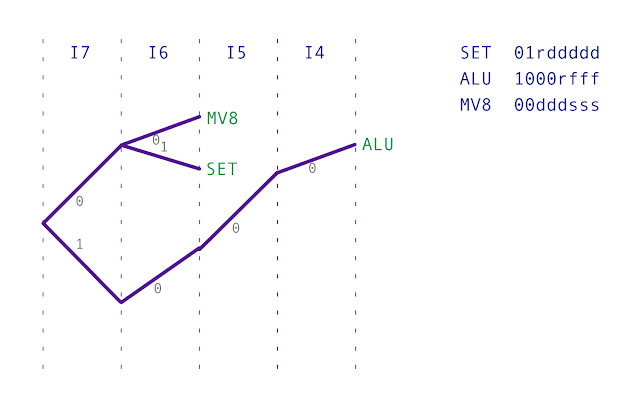
There will be further branches to this tree in the future as more instruction classes are added to the computer but for now I’m keeping to the three above as that will be enough to perform some simple programs. The tree above can now be easily mapped to the relays used by this computer:
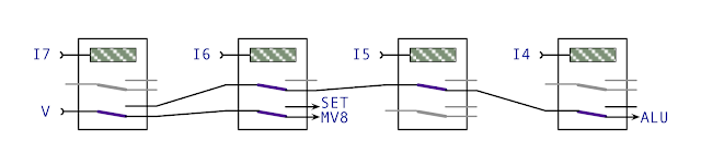
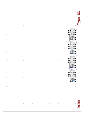
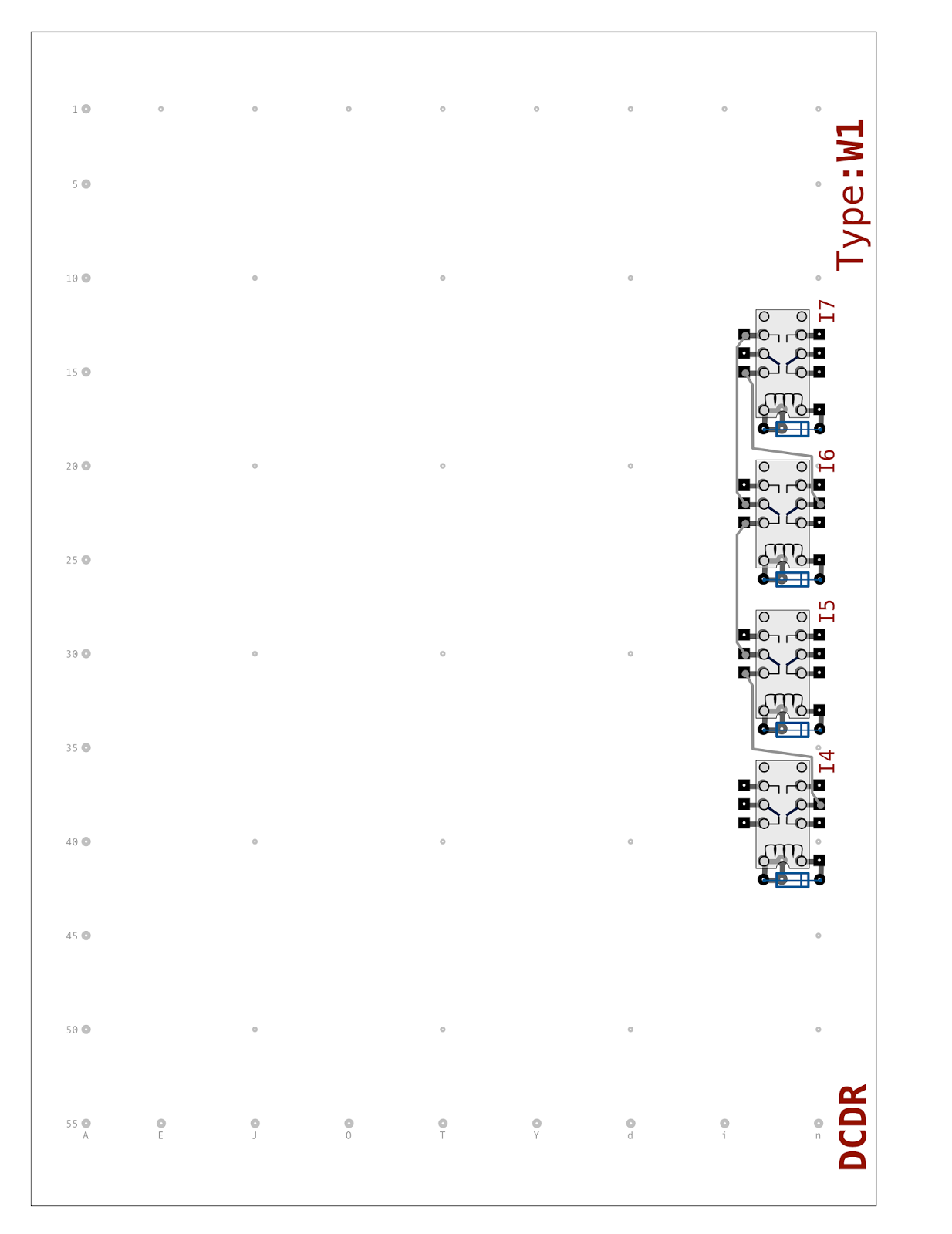
With the basic relay connections designed it’s time to transfer this over to a 55 x 40 hole pad board as used on all the computer cards so far.
As usual I’ll want the card to display the current instruction class being decoded so I can confirm correct operation and test/debug the card independantly. 3 LEDs will be needed for this to handle the three classes currently decodable and as always these are the 12V LEDs with internal resistor. Diagram wise it looks like this:

The mysterious gap between the MOV8 and ALU LEDs above is where a later instruction class LED will go (and there’ll be more LEDs added to the right as the card gets more classes added).
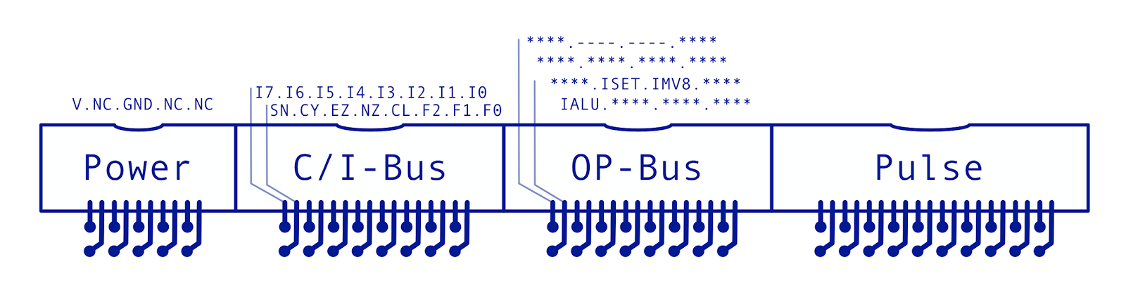
Next up is the connections to other parts of the computer and there’s yet another new connection type to introduce again … and this one is a little odd. So far I’ve introduced the ’type Z’ connections (used on the three ALU cards and the AD and BC register cards) and the ’type X’ connections (used by the instruction register covered in my last post). The enclosure which holds the cards has five type Z slots and five type X slots. There will be ’type Y’ connectors which will be used by upcoming cards but these are again pretty similar to the type X and Z cards and the enclosure can hold five Y cards too. This card however is a ’type W1’ and the enclosure can hold three ’type W1’ cards and two ’type W2’ cards. The reason for this oddity is because some of the W cards will be double height to use both W1 and W2 connectors but for now we can think of W1 cards just like any other X, Y or Z cards. As you might expect any W1 card can talk to any other W1 card on all the available connection lines.
The ‘W1’ connections consist of the pulse timing signals (which will be produced by the upcoming sequencer card), 8-bit control & instruction bus, 8-bit operation bus and finally power connections. The diagram of the connectors look like this:
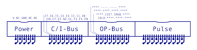
This shows the four right angled boxed headers — from left to right these are: 5+5 power lines, 8+8 control/instruction bus, 8+8 operation bus and finally 10+10 pulse lines. On the operation bus the lines marked ‘***’ are lines that will be used by future ‘W1 type’ cards and the lines marked ‘—’ are unused/spare. The pulse lines are not labelled at the moment but that will all be changed when I design the upcoming sequencer card. The lines on each connector are as follows:
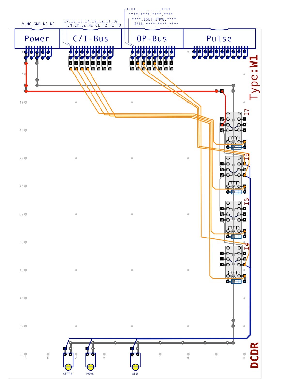
So, finally, wiring everything together we get the following:
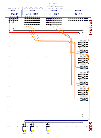
This diagram includes everything mentioned so far along with the power supply and ground lines and all other internal wiring. As with previous cards, the completed decoder design can be found here in PDF format.
So, that’s the decoder all designed and ready for the first three instruction classes. The next card to design is the sequencer which will produce the timing pulses that the control card (which I’ll design after the sequencer) will use along with the instruction class produced by this card to fire the control lines in the required order. When all of that is done it’ll finally be time to get constructing and put together these four cards (instruction register, decoder, sequencer and control) which will get the computer to the stage where a single instruction can be performed fully by manually pulsing the clock line.