Well, it’s fair to say that I rather underestimated just how much time decorating the new house would take up … and that’s mainly because ‘decorating’ included re-wiring, re-plumbing, re-plastering, re-carpeting … all before I got anywhere near choosing a tasteful shade of emulsion for the walls. Needless to say then that spending time on my relay computer has suffered quite a bit. However, things are starting to calm down (now that there’s two rooms in the house that are semi-habitable) so I can get back to designing the next bits for the computer.
The next card up for design is the (mercifully straightforward) 8-bit instruction register. I say straightforward as this card shares much of its design with the B/C register card already constructed. The instruction register is permanently connected to the instruction bus just as the B/C registers are permanently connected to the ALU. However where the B/C registers are general purpose, and so can be set from and selected to the data bus, the instruction register can only be read from the data bus.
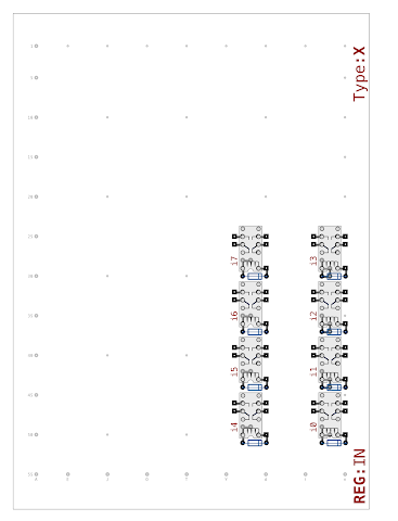
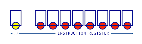
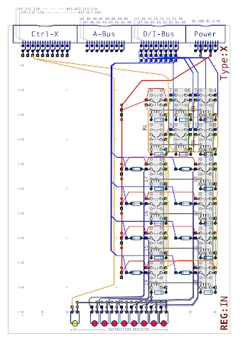
So, as I’ve done in previous design posts, I’ll start with a card schematic of what the main bit relays look like for the 8-bit instruction register when placed on the usual 55 x 40 hole pad board (excluding wire links):
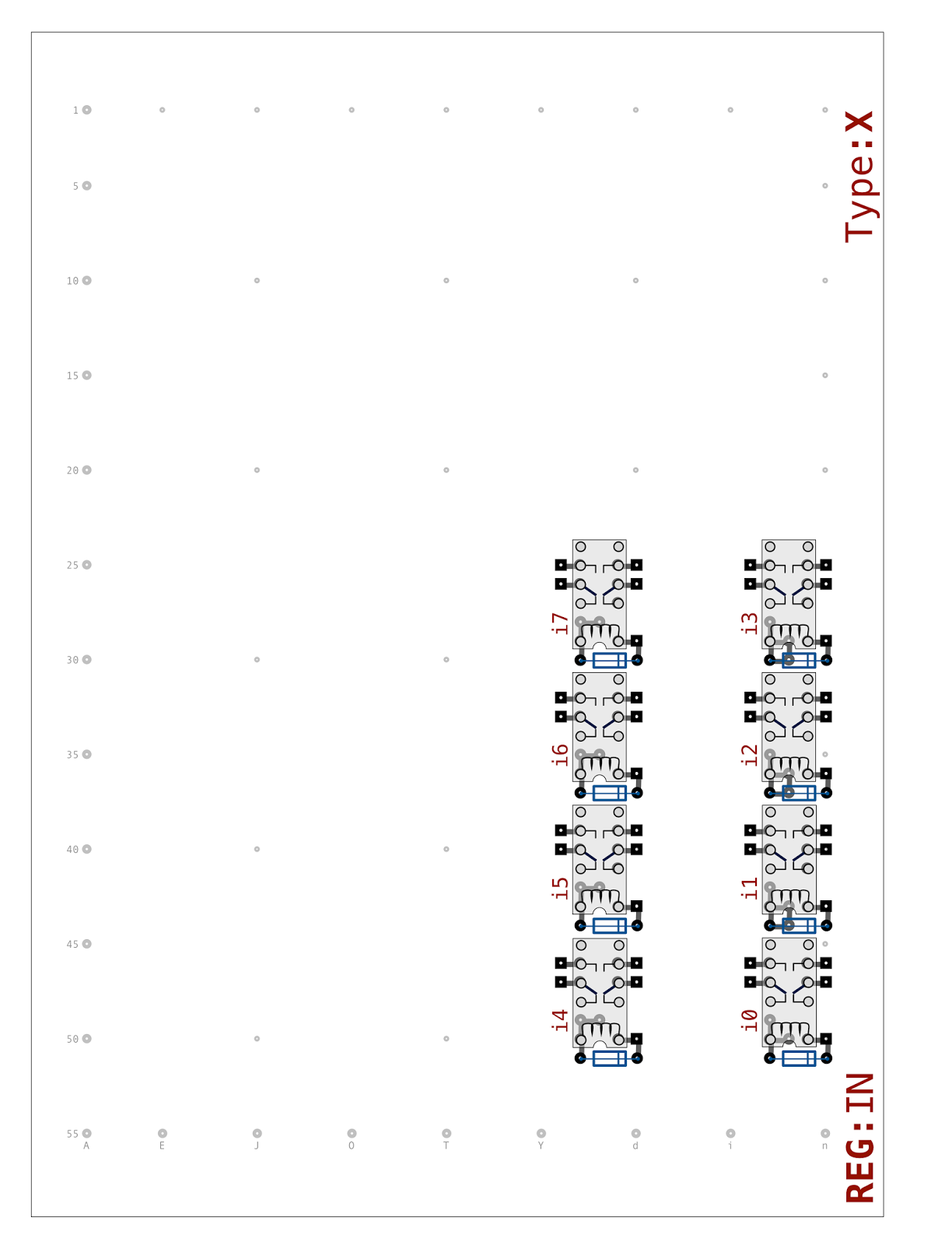
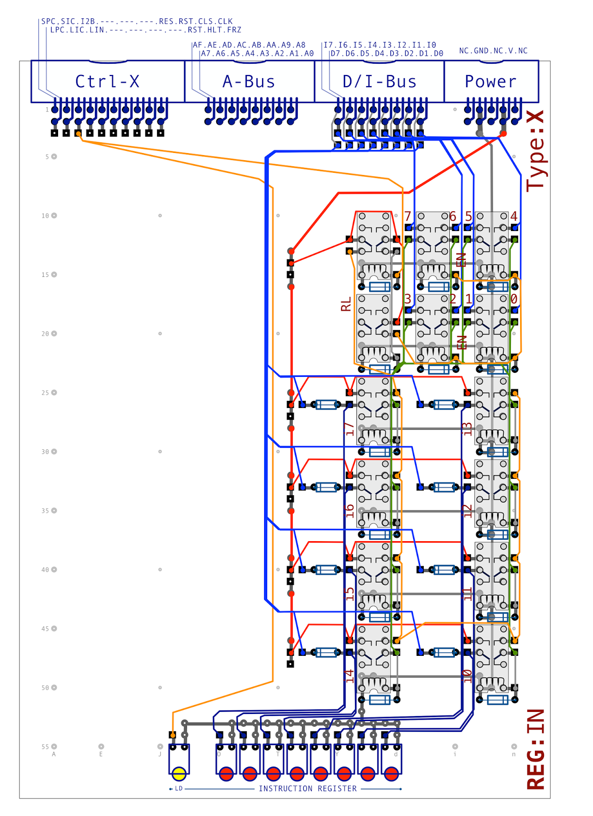
Each of the relays above stores a single 1-bit value so there’s 8-bits worth in total. Each of the bit relays need gating from the data bus so the register can be loaded when required. With these additional control and gating relays added we get the following (this time including internal wire links in the 1-bit register relays and result links between the 1-bit register relays and the gating relays):
Additionally on the schematic above you can see there’s an extra diode per register bit relay — this is where the register bit permanently feeds the instruction bus and the diode ensures that the bus can’t accidentally back-feed into a bit relay. Actually, in this case, if the diodes weren’t there and back-feed did occur then the only effect would be a garbled LED display due to display of the real register value combined with the back-fed value. As things currently stand the instruction bus is only driven by this register and would never be in a position to back-feed anyway but the diode ensures this register card protects itself from any outside influences. There is, of course, a voltage drop across the diode to keep an eye on when I get to the design of the control card which will use further diodes to make up some of the combinatorial logic … the risk being that if the voltage drops too low any target relays may fail to switch properly. The relays I’m using (TE Connectivity V23079A2003B301) are 12V but the coil can operate as low as 9V so given the 1V drop of the 1N4148 diodes I’m using I should be able to safely get 2 diodes in line before things get dicey. If I do get in trouble later I can either pop in a ‘relay’ relay downstream to pass the signal on and get the voltage back up to 12V or I can wire link over the diodes on this card and accept the risk of back-feed.
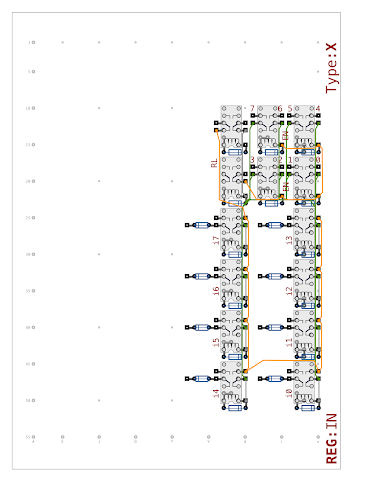
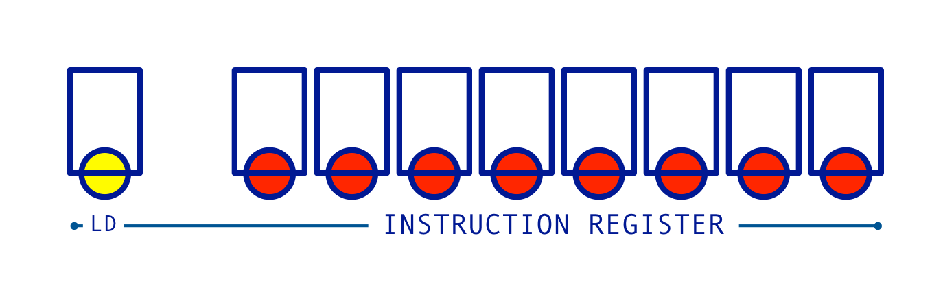
Relay wise that’s it for this card. As with all the register cards designed so far I’d like to display the current value being stored in the register (even though the same value is always present on the instruction bus). This allows me to confirm correct operation and test/debug the card independently. For this 9 LEDs are needed … 8 for the bit register values and 1 to show when the register is being loaded from the data bus. The LEDs are the same 12V ones used in all the previous cards (with an integral resister). Colour wise I’m continuing with the theme of red for a bit value and yellow for control signals. Diagram wise it looks like this:
Each block in the diagram represents a single 3mm LED in a plastic holder with each LED pushed into the holder from the front and the pair of LED legs then bent at 90 degrees.
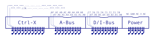
Next up is the connections to other parts of the computer and there’s something new this time. All the cards designed so far have been marked ’type Z’ and they share a common set of connectors on the back of the card such that Z cards can talk to each other directly as needed. There are five Z cards which fit in to the corresponding Z backplane that sits in the lower left bay of the enclosure. The instruction register card requires slightly different connections (like the instruction bus) and doesn’t need some of the Z connections (like the B/C bus) so this card will be a new ’type X’ card. As you might expect X cards can talk directly to other X cards via a new X backplane and the X and Z backplanes have their common connections (like the data bus) hooked up together to allow them to talk to each other.
The ‘X’ connections consist of the 8-bit data bus, 16-bit address bus (to be used by future X cards), 8-bit instruction bus, power connections and finally the control signals to load this register. The diagram of the connectors look like this:
This shows the four right angled boxed headers — from left to right these are: 10+10 control lines, 8+8 address bus, 8+8 data and instruction bus and finally 5+5 power lines. On the control connector the lines marked ‘***’ are lines that will be used by future ‘X type’ cards and the lines marked ‘—’ are unused/spare. The lines on each connector are as follows:
- Ctrl-X (Control Line Bus)
- LIN … Instruction Register Load
- A-Bus
- A0-AF … 16-bit Address Bus
- D/I-Bus (Data Bus + Instruction Bus)
- D0-D7 … 8-bit Data Bus
- I0-I7 … 8-bit Instruction Bus
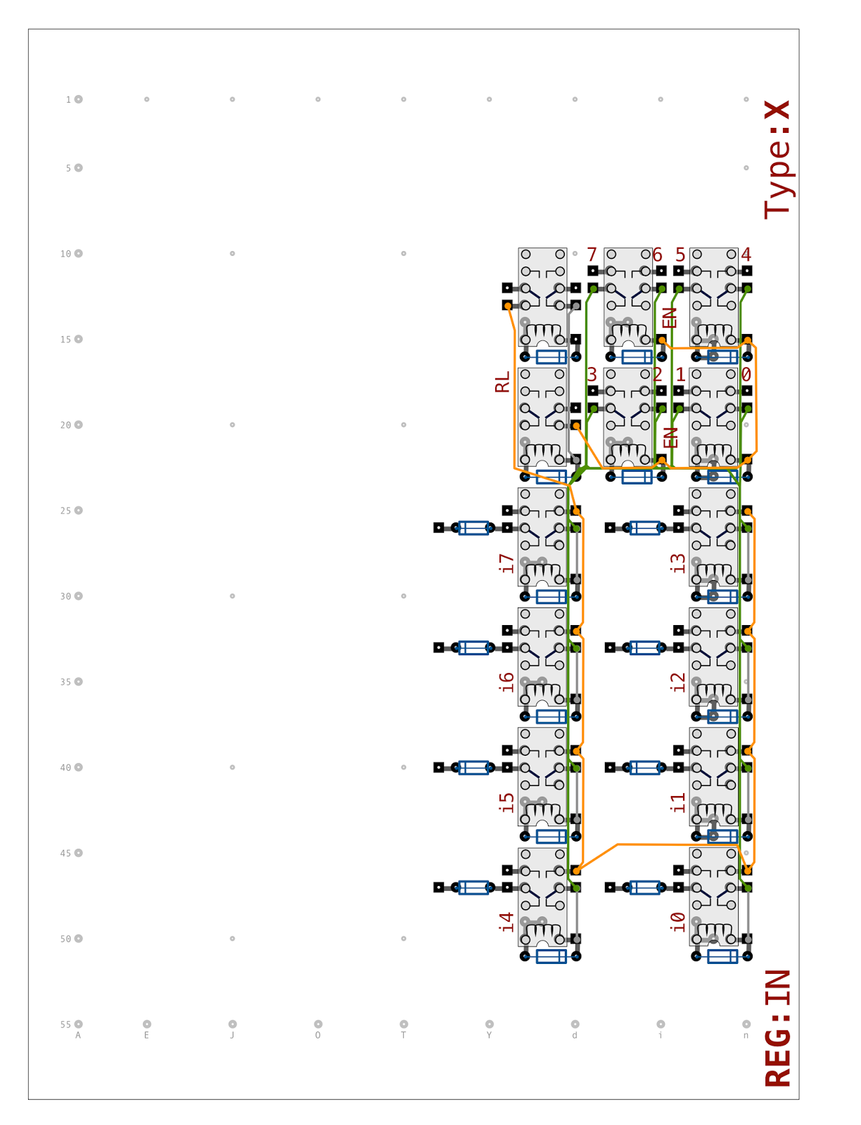
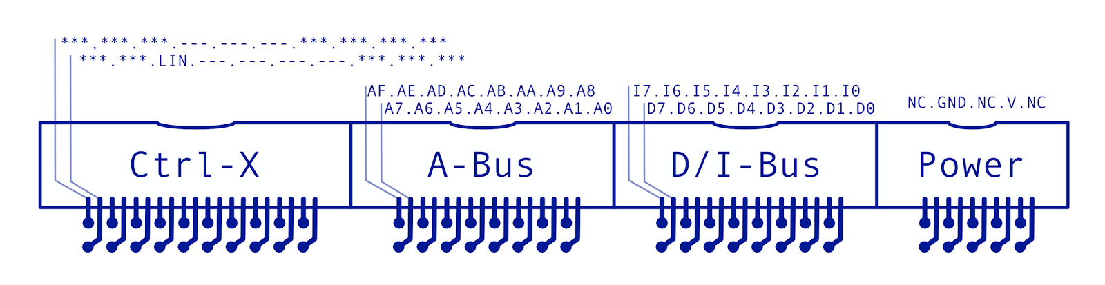
So, finally, wiring everything together we get the following:
This diagram includes everything mentioned so far along with the power supply and ground lines and all other internal wiring. As with previous cards, the completed instruction register design can be found here in PDF format (so you can zoom right in on the detail).
So, that’s the instruction register all designed and ready for construction however as I’ve still not got anywhere suitable for soldering in the house just yet that’ll be on hold for a bit. In the meanwhile though there’s plenty more cards to design and the next one in line is the decoder. This card will take the value on the instruction bus and decode what class of instruction that value represents. Following that card I’ll design the sequencer and control cards introduced in my last post. When all of that is done it’ll finally be time to get constructing and put together these four cards which will get the computer to the stage where a single instruction can be performed fully by manually pulsing the clock line.