ALU Operation
Performs an arithmetic or logic operation on the B (and optionally C) register(s).
  r = destination register (0-A, 1-D)
fff = function code (000-NOP, 001-ADD, 010-INC, 011-AND, 100-OR, 101-XOR, 110-NOT, 111-SHL)I’ve now got my computer to a state where I can perform ALU operations and push values around the four registers by manually operating the various control lines. It’s time to move things on a bit now and work towards getting the computer to the point where given a specific instruction/op-code it can operate the control lines itself without further input from the user. Eventually the computer will be given a list of instructions to perform which it’ll work through step by step but for now the next milestone is to automate the operation of a single instruction.
In my recent videos I’ve been demonstrating, by hand, the processing of a simple arithmetic sequence on the computer by following a list of instructions represented as a set of mnemonics. Here’s a screenshot from the video showing the full set of mnemonics/instructions to perform the calculation of (((2 + 4 + 1) x 3) - 3):
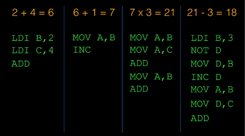
Here’s a description of the mnemonics used in this calculation:
| Mnemonic Form | Instruction Class | Description |
|---|---|---|
LDI r,v | Load Immediate | Loads the value v in to register r |
MOV s,d | 8-bit Move | Copies the value in register s to register d |
ADD | Add | Performs an ALU ADD operation placing the result in register A |
INC | Increment | Performs an ALU INC operation placing the result in register A |
NOT | Logic Not | Performs an ALU NOT operation placing the result in the register A |
One thing I should mention here is that although these mnemonics are fairly common I’ve introduced a bit of an inconsistency with the MOV instruction which should really have the destination parameter first followed by the source parameter so that it matches the LDI instruction. Some assembly languages have source first then destination, some have it the other way around but all instructions should at least be consistent. Eventually I’ll slip this change in so that the instruction will become MOV d,s.
There is, of course, other operations the ALU can perform and the mnemonics for these would be:
| Mnemonic Form | Instruction Class | Description |
|---|---|---|
AND | Logic And | Performs an ALU AND operation placing the result in register A |
ORR | Logic Or | Performs an ALU OR operation placing the result in register A |
XOR | Logic Exclusive Or | Performs an ALU XOR operation placing the result in register A |
SHL | Bitwise Shift Left | Performs an ALU SHL operation placing the result in register A |
Although all the ALU operations shown here place their result in register A by default you can optionally specify either register A or D, as a parameter, to change where the result is placed. All of the ALU operations also load the condition register whilst the result is on the data bus.
The mnemonics shown above are, as the name suggests, a handy way to remember the underlying 8-bit opcode (binary instruction) that the computer understands and can operate from. The mnemonics introduced so far fall in to three broad classes: ALU, SETAB (Load Immediate) and 8-bit MOVE operations. The opcodes are as follows:
Performs an arithmetic or logic operation on the B (and optionally C) register(s). Copies the content of one 8-bit register to another. Loads a value between -16 and +15 in register A or B.ALU Operation
r = destination register (0-A, 1-D)
fff = function code (000-NOP, 001-ADD, 010-INC, 011-AND, 100-OR, 101-XOR, 110-NOT, 111-SHL)8-Bit Move
ddd = destination register (000-A, 001-B, 010-C, 011-D, 100-M1, 101-M2, 110-X, 111-Y)
sss = source register      (000-A, 001-B, 010-C, 011-D, 100-M1, 101-M2, 110-X, 111-Y)
Load Immediate
    r = destination register (0-A, 1-B)
ddddd = value (-16..15)
Designing these opcodes is all about fitting enough options in to the bits available whilst still being able to distinguish one instruction class from another. As you can see above, any instruction starting with 1000 must be for the ALU whereas any starting with 00 must be about moving (or more precisely, copying) data between registers. As MOV-8 instructions only use two bits to identify that class of instruction there’s enough room to allow the selection of eight different registers for both source and destination. In contrast, the ALU only needs three bits to pick the ALU operation to perform so it’s then a toss up between having more instruction classes or limiting the destination where the ALU result can be placed (in this case 1 bit is used for the destination parameter and four are used to identify the class of instruction).
There will, of course, be more instruction classes to come in time but for now the ALU, SETAB and MOV-8 are the ones I’m going to concentrate on. Before I go any further I should mention that the instruction set I’m using is directly based on that used in the relay computer by Dr Harry Porter which was then expanded on by Phil Ryals at the Goodwill Computer Museum on the RC-3 relay computer.
Each mnemonic I use has an exact opcode equivalent and some examples of these are listed below (effectively a list of all the unique mnemonics used in the arithmetic sequence at the top of this post). Once the computer is complete I will generally write programs for execution as a list of mnemonics (which are easier for me to remember) which can then be ‘assembled’ line by line in to a list of opcodes (which are something the computer can work with).
LDI B,2   [SETAB]   01100010
LDI B,3   [SETAB]   01100011
LDI A,4   [SETAB]   01000100
ADD       [ALU]     10000001
INC       [ALU]     10000010
INC D     [ALU]     10001010
NOT D     [ALU]     10001110
MOV A,B   [MOV-8]   00001000
MOV A,C   [MOV-8]   00010000
MOV D,B   [MOV-8]   00001011
MOV D,C   [MOV-8]   00010011
Now, again, I’ve messed up a bit again in the mnemonics I’ve used for that arithmetic sequence … I’ve used a LDI C,4 which actually doesn’t have an opcode equivalent because the SETAB class of instruction can only load the A or B register (not C). I can resolve this by loading the value in to register A with a LDI A,4 and then copy the value in to register C with a MOV-8 class of instruction.
So, as far as designing cards for the computer to handle the processing of these opcodes goes the first jobs are to store the instruction and then decide which class of instruction it represents. Storing the instruction is easy enough and is achieved by adding another 8-bit register which can be loaded from the data bus. This ‘instruction register’ is pretty similar to the general purpose registers introduced so far but has its current value hard wired to the decoder and control circuits. The decoding circuit is also quite simple and should need only around five relays to handle the logic of deciphering the instruction class from the higher five bits of the instruction code. For the instruction classes introduced so far (SETAB, ALU and MOV-8) that logic is as follows:
This will all be implemented on a new ‘decoder’ card. This card will be fairly barren given how few relays are required to handle the decoding logic but none of the other cards will really have enough spare space so c’est la vie and all that.
Now that we have the instruction code in hand and can work out which class the code belongs to the next job is to operate the appropriate control lines in sequence. For each instruction class these are the steps to take:
Visualising these as timing diagrams we get the following:
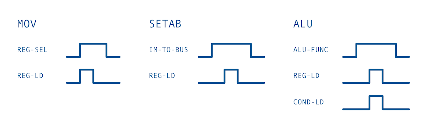
As can be seen in the diagram above the value being copied (or calculated for the ALU) is kept on the data bus longer than it is loaded in to the destination registers. This is to allow the value to ‘settle’ on the data bus and avoids issues where the source relays may turn off quicker than the destination relays hence loosing the desired value. All mechanical switches also suffer from an issue known as ‘bounce’ where the contacts connect and disconnect rapidly before settling down when set on and this is also what the overlap allows for.
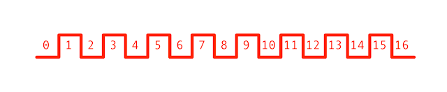
Although these timing diagrams look quite simple there’s actually quite a lot of infrastructure required to produce these in a relay computer. You can probably see from the diagram that there is three distinct shapes of pulses … the single pulse used in all three commands, the double pulse in the MOV command and finally the triple pulse in the SETAB and ALU commands. How can these be produced? Well, we need to start with something quite simple … a heartbeat that the entire computer will run from.
That heartbeat is known as a ‘clock’ and it produces a steady on/off train of pulses that can then be combined and have simple logic gates applied over to get the desired timing signals. My computer will actually have two clocks … one which is made out of a chain of relays and capacitors to make an electromechanical clock that runs at a fixed rate and a second one that uses the popular 555 timing IC that will be variable. The former clock is more ‘in keeping’ with the design of a relay computer but I wanted to be able to switch over to a variable clock that has the flexibility of speeding the computer up or down as required/desired. Also the variable clock will be far quieter than the ‘chattering’ fixed clock which again further aids the choice between authenticity and practicality (the rest of the computer will then, of course, still happily click away without being drowned out by the clock relays). Either way the timing diagram for the clock will always look as follows (with evenly timed on and off periods) regardless of relay/IC selection:
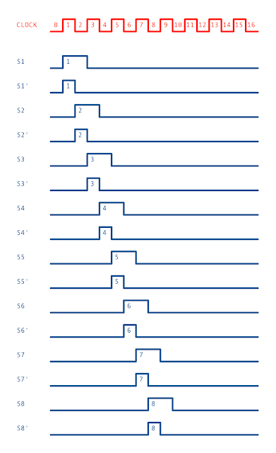
The first step in using these clock pulses is to achieve a sense of state in the computer. Effectively we need to count the clock pulses so we can tell if we’re at the beginning, middle or end of an instruction. This is implemented using a Finite State Machine (FSM) which will effectively count up the clock pulses reseting at predetermined points (when the instruction is complete). Eventually the FSM will count up to a maximum of 23 for the more complex instructions and will be resettable at stage 8, 10, 12 and 14 for instructions that require less steps. The SETAB, ALU and MOV-8 instructions can all be handled within 8 steps so for now we’ll stick with an 8 step FSM.
The FSM gives out a series of pulses according to the step it is currently on. For each step there is typically a pulse that lasts a single clock cycle and one that lasts two. This will come in useful later when combining these pulses to avoid any gaps in the resulting pulse that could cause erratic behaviour. The timing diagrams for the first eight steps is as follows:
Given these outputs from the FSM we can now apply the following logic to derive those three pulses needed to implement the MOV-8, SETAB and ALU instructions:
Shown as a timing diagram these pulses combinations look like
this: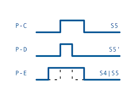
Now, this diagram probably raises more questions than it answers. Firstly, why is the first pulse named ‘P-C’ … surely there is a ‘P-A’ and ‘P-B’ … there is indeed and these will be used later on to load and increment the program counter and to load the current instruction from memory in to the instruction register. This is also why the C, D and E pulses are based on state 4 and 5 on the FSM because the earlier states drive the preparation of the instruction register.
Implementation wise the FSM and sequencing pulses will be handled on a pair of sequencer cards which will take the clock pulse and generate a full set of sequence pulses. Again, for now, I’ll only be concentrating on producing P-C, P-D and P-E but eventually there’ll be a full range of pulses to implement all the various instructions the computer will be capable of performing.
So, with the sequencing pulses and operation class in hand it’s now just a case of implementing fairly simple relay logic gates to direct these pulses to the appropriate control lines at the right time. This will take place on the ‘control’ card and as with the other cards this will eventually handle the direction of the full set of pulses to the right control lines for all instructions.
That’s pretty much it for sequencing and control in theory. The next step now is to begin designing the cards that will make all this a reality for the MOV-8, ALU and SETAB instructions. These cards will be:
For the moment I can get away without the clock card as I can manually produce the clock pulses using the ‘CLK’ toggle switch on the computer front panel but once everything is looking good and working that’ll be the next card to create.
In my next post I’ll cover the design of the instruction register and following that I’ll run through the design of each of the cards listed above. Once all four cards are designed I can get on with the construction and testing … all being well this will coincide with my new house having all the decorating and so on complete and I’ll have somewhere to actually get on with constructing the cards.