Following on from working on the main data switches in my last post this time I’ve taken the first steps in designing and constructing the first of two display cards which will sit in the upper enclosure. The first card (display A) has a dual purpose … it provides a display to show which control signals are in operation between the various parts of the computer but also allows the operator to manually control those signals when the computer is set to a special ‘diagnostic’ mode.
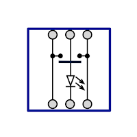
As with the data switches I knew all along what type/style of components I wanted to use to act as a display and switch over a single control line … in this case I’ve specifically gone for the NKK JB series which are illuminated tactile switches. These are momentary switches and available in either red, green or yellow (I’ll use all three colours in the final display). The switches are X/Y stackable so it’s quite easy to make keypad type layouts with them. Internally the switches are laid out like this:
For each switch I’ll need to apply a label of some kind to indicate its function and this is where I can draw on some prior experience. My first job after leaving school at 16 was at a screen printing company in the reprographics department. This was around the point where computers were only just starting to be used in this industry and so I still did a lot of work by hand with pens, rulers and … more relevantly to this post … letraset (which is a sheet of transferrable lettering). This is perfect for my needs and fortunately (and quite surprisingly) it’s still available albeit in a limit range of fonts, sizes and colours (back at my first job there were huge catalogues of available styles). With the letraset applied to one of the JB key caps it looks like this:
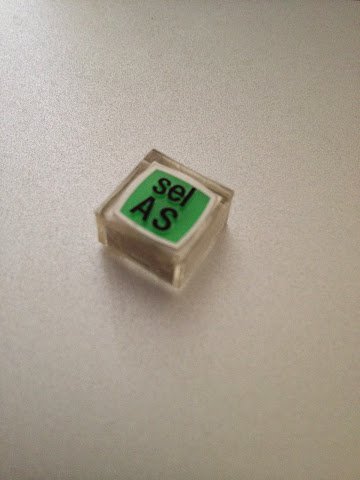
I’m quite pleased with how these look even though the lettering is a bit wonky (all part of the charm I guess). However, I’ve had to cheat a bit … the key cap as it appears above is made of two parts: the outer clear lens and an inner white body … apparently the two can be separated but I’m damned if I can do it without chewing up the plastic so I’ve applied the lettering directly to the lens and then covered it with sellotape (neatly folded around the corners) to protect it. If I ever do work out how to remove the caps I can always do it properly later on … and I know the tape and lettering comes off cleanly as I had to redo a couple of caps where I’d forgotten they only fit on to the switch base in one direction (so the lettering ended up rotated 90 degrees from where it should have been).
With the switches selected
and a method of labelling them tried and tested it was time to design the
display board itself. As with the switch control board shown in the last post
this board has gaps in it where more functionality will be added later on.
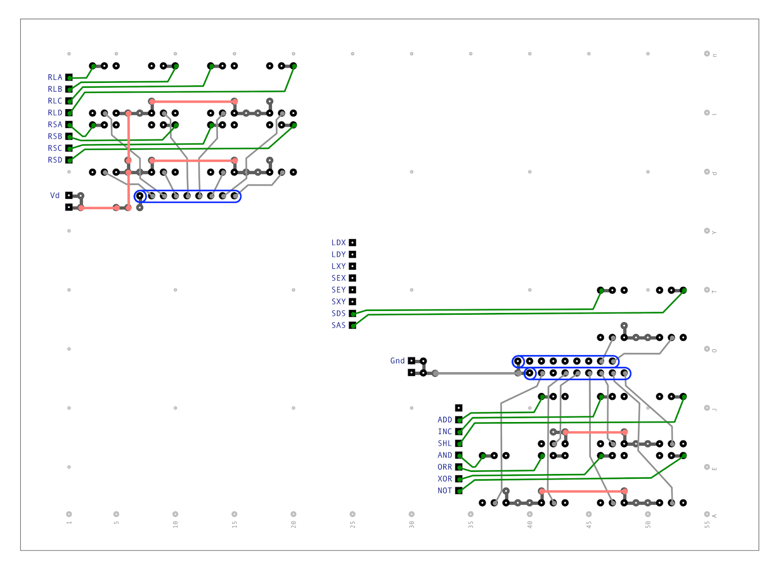
This is the design so far with key caps on: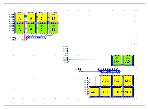
The upper left set
of eight switches control and display the A, B, C and D register load and
select lines. The lower right set of seven switches control and display the
ALU operations. Finally the two switches above those control and display the
gating of the data switches on to the data and address busses respectively.
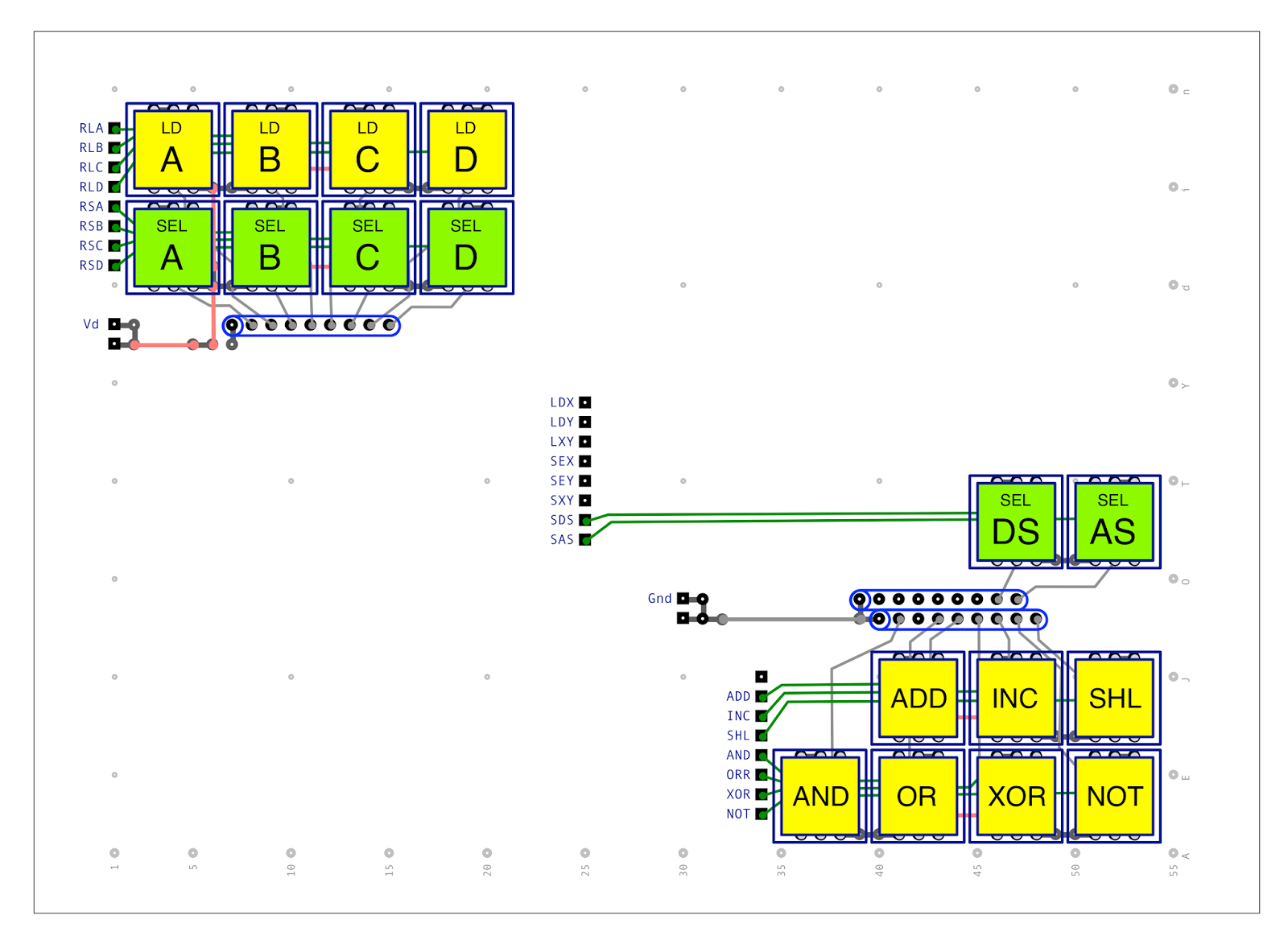
The same diagram with switches removed looks like this: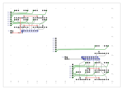
The control signals come in (and go out on) the three sets of header pins to the left of each switch group. These header pins will protrude from the back of the card so that a ribbon cable can be attached that heads off to another card where it’ll be wired out to the various busses of the computer. The top middle and bottom middle pins of each switch carries the illumination LED (anode at the top) and so from the bottom middle pin a connection to ground is made via a 560 ohm resistor (which is packaged in an eight resistor array). These means if a signal is coming in on a control line it will light the LED regardless of switch position. When the switch is pressed however it will link the power supply (which is only active when the computer is in the diagnostic mode) with the control line and the LED.
As always these schematics are available in PDF format here for the schematic with switches and here without the switches.
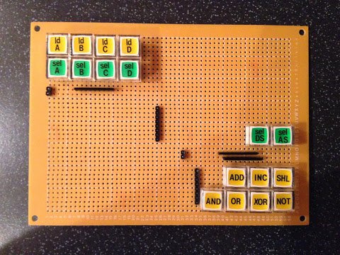
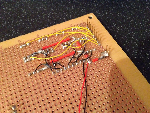
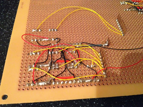
So, with the design ready to go I could get out the soldering iron and get stuck in. The only real change from previous cards is that all the wiring is done on the back side of the card this time with soldered Kynar wire. Other than that there’s nothing too surprising or unusual in the construction so I’ll get straight on with the pictures. Here is the card as it currently stands viewed from the front:
… and from the back …
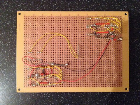
… and finally here’s a couple of close up pictures focussing on the upper right and then lower of the back of the card …
… and that’s it for now on this card. I’ve tested everything lights up properly and I’ll put a video together showing everything working after I’ve constructed the first parts of the second display card and wired everything in to the main computer cards.