In my last post I put together the beginnings of the first display card … named in a brilliant flash of nomenclature as display card A. This time I’m turning my attention to the second display card … named (can you guess) display card B.
Whereas display A is dual purpose allowing a user to view and initiate control signals the second display card is read-only and displays the primary state of the computer. Initially this ‘primary state’ comprises of the data bus contents, condition register status and ALU function code / operation. I also had a rectangular gap spare on the card that looked like it’d fit an ammeter so that also now forms part of the second display too.
As with the display A buttons and the primary input switches I’ve known what kind of display elements I wanted to use right from the beginning. Taking inspiration from a visit to the National Museum of Computing in the UK I fell for the big chunky buttons/indicators on the ICL 2966’s ‘washing machines’ / storage units. Here’s an example of my interpretation of that retro look:
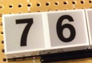
Here I’ve applied a nice chunky letraset font directly to the faces of an Avago light bar unit. These units come in a variety of bar shapes so that within the same package outline the face area is divided in to one, two or four discrete lit segments. Each package lights up green, yellow or red (all segments within a package the same colour) and although the ones above are red they appear the same milky white colour until actually lit. Finally, these units are also X-Y stackable so it’s quite easy to build up complex displays.
With the selection of display units in hand I’m now able to design the display card itself. As with display card A I’m only sharing a partial design for this card … effectively as much as I’ll actually be constructing. Eventually the gaps on this card will be filled by yet more indicators for the various bits of the computer I’ll add in the future. This is more about constructing the bits I need when I need them and saving money on parts until I’m ready for them rather than teasing my audience (if anyone really, really would like to see the complete design for any of these partial cards drop me a line in the comments and I’ll be happy to share). Anyho, here is the design with indicator faces shown:

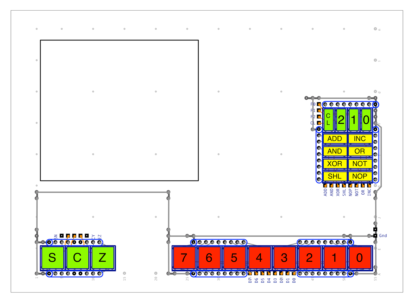
The lower left indicators show the condition register status (Sign, Carry and Zero). The lower right indicators show the current value on the data bus. The upper right indicators show the ALU function code along with the decoded ALU operation and also the Condition Register Load line. Finally there’s the rectangle in the upper left of the card that marks the outline of the ammeter. The same diagram with the indicator faces removed looks like this:
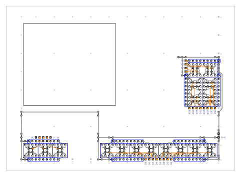
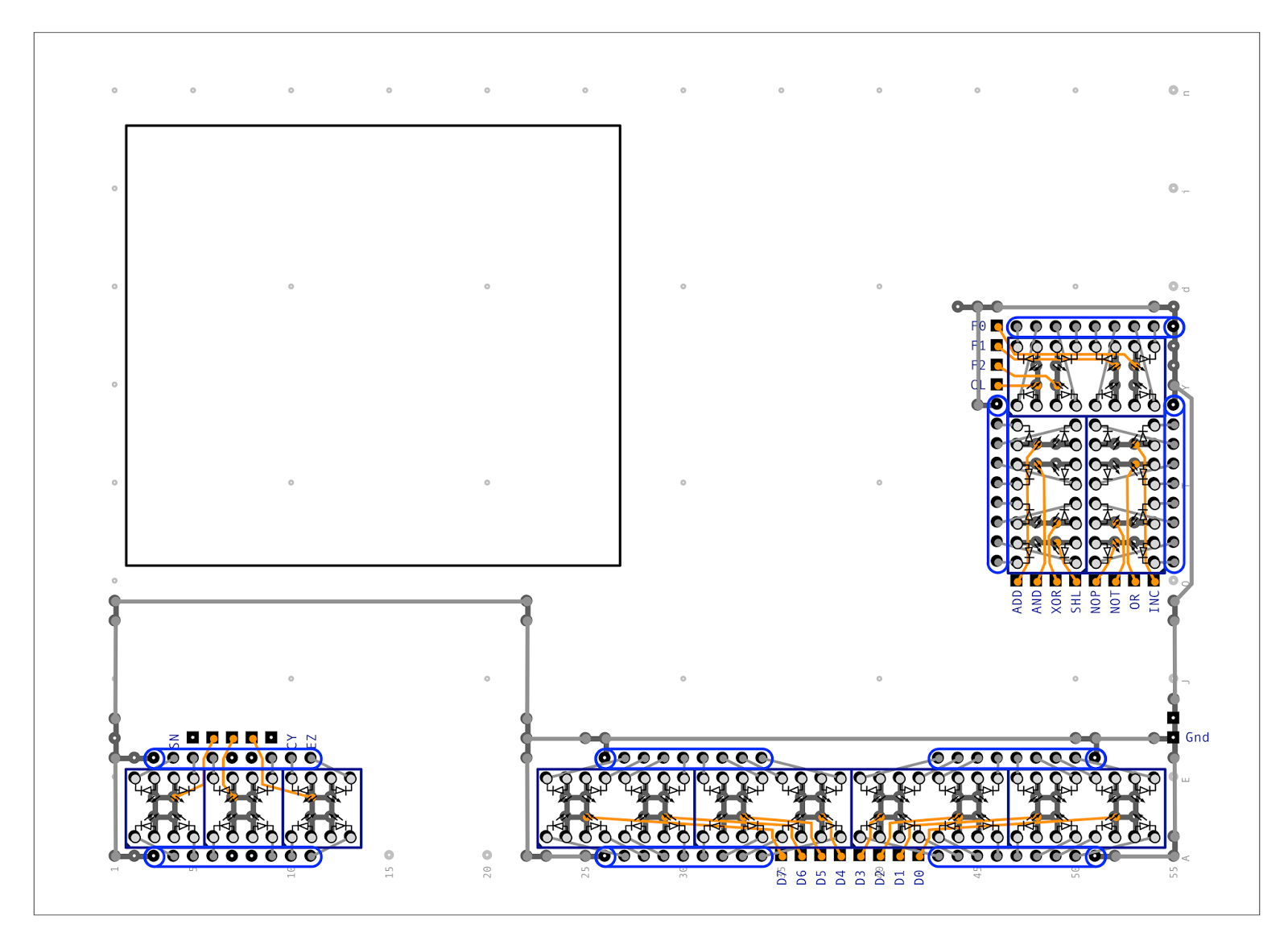
If you look at this diagram close up (you can click the picture above to view a larger version) you can see that each of the indicator units has the same internal layout of LEDs which makes wiring up much easier. Each LED anode is connected to the appropriate header pin bringing in the signal from the rest of the computer. On the cathode side of each LED is a single 1K resistor packaged up in an array of eight resistors. This is higher than the 560 ohm resistor used on the display A buttons to try and match the light levels a little better (running these units at their rated current was way too bright and actually a bit unpleasant to look at … bringing them down with a 1K resistor made them just about right).
As always these schematics are available in PDF format here for the schematic with indicator faces and here for the schematic without.
So with the design all done I can move on to making the card for real. Technique wise there’s nothing really new compared to constructing display card A although I have put in some DIL sockets to carry the display units just in case I ever need to replace them or tweak anything. To fit the ammeter I made a paper template first and then marked out the area on the card / pad board and drilled some pilot holes. From there I attempted to cut out the hole with a junior hacksaw but didn’t get very far so I resorted to nibbling away at the board with a pair of pliers which actually worked very well. Here’s the card as it currently stands from the front:
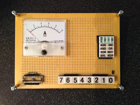
The condition register display units aren’t shown here on this picture as they were out of stock when I ordered them so arrived after this picture was taken (originally these were going to be red indicators but it was a 6 week wait for those so I switched out for the green equivalent which actually ended up looking better). The four spacers with screws in each corner of the card are a temporary addition which allows me to work on the back of the card without scratching the front of the card to bits. Speaking of the back of the card … that looks like this:
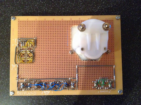
Here’s a couple of close up pictures of the card back:
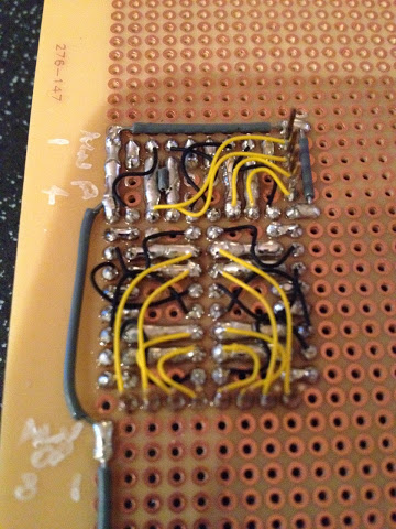
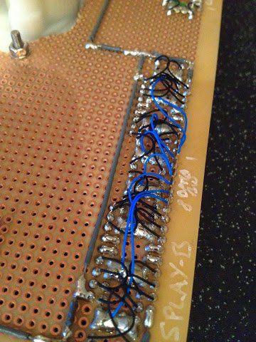
… and here’s a couple of close ups on the indicator units …

… and that’s it for now on this card. I’ve tested everything lights up correctly but I’m not posting any photos of that just yet - I’ll leave that for the next post when I hook up the primary switches and display A and B to the rest of the computer and give it a whirl. I’ll also produce another video (don’t groan) showing everything built so far working fully.