In a recent post I put up the design for the A and D 8-bit register card … the B and C register card is very similar in design but has the additional complexity that it has to directly feed the ALU. In another recent post I covered how to take multiple outputs from a relay without risking back-feed by utilising diodes in the output line. This post therefore brings together those two designs and although it’s essentially a re-hashing of the AD card post but with extra bits I’ll go through the design as I did with the AD card so that this post stands alone as it were.
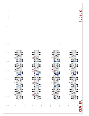
So, as before, I’ll start with a card schematic of what the main bit relays look like for the two 8-bit registers when placed on the usual 55 x 40 hole pad board (excluding wire links):
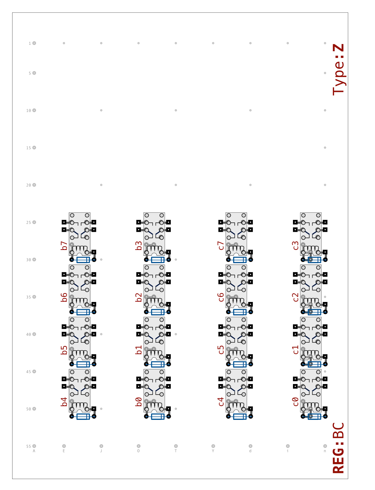
Each of the relays above stores a single 1-bit value so there’s 16-bits worth in total (which could all be used together if we were making a 16-bit register) or two lots of 8-bits (for our two 8-bit registers). Each of the 1-bit register relays need gating to and from the data bus so that the values stored don’t conflict with any other value on the data bus. With these additional control and gating relays added we get the following (this time including internal wire links in the 1-bit register relays and result links between the 1-bit register relays and the gating relays):
Additionally on the schematic above you can see there’s an additional diode per register bit relay - this is where the B/C feed to the ALU will be taken from and the diode ensures that the ALU can’t accidentally back-feed into a bit relay. Actually, in this case, if the diodes weren’t there and back-feed did occur then the only effect would be a garbled LED display due to display of the real register value combined with the back-fed value. As things currently stand the ALU would never be in a position to back-feed anyway but the diode ensures this register card protects itself from any errant outside influences.
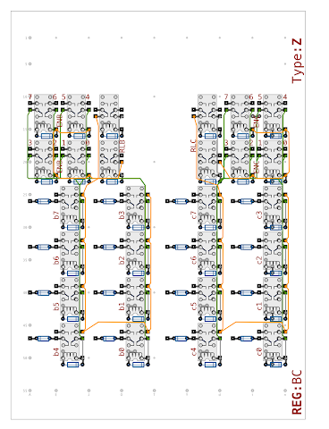
So, relay wise, that’s it for this card. As with the AD register card I’d like to display the current value being stored in the registers regardless of the whether that value is being gated on to the data bus or not. This allows me to confirm correct operation and test/debug the card independently. For this 20 LEDs are needed … 8 for each of the two 8-bit register values, 2 to show when each register is being loaded and finally 2 for when each register is being gated on to the data bus (selected). Fortunately there’s just enough room down the front of the card to fit in the 20 LEDs required in single row LED holders and so this also simplifies the wiring behind the LEDs. The LEDs are, as always, the same 12V ones used in all the previous cards (with an integral resister). Colour wise I’m continuing with the theme of red for a bit value, yellow for inputs or control signals and green for output control signals or state. Diagram wise then it looks like this:
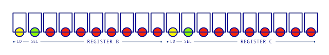
Each block in the diagram represents a single 3mm LED in a plastic holder. Each LEDs is pushed into the holder from the front and the pair of LED legs are bent at 90 degrees.
Next up is the connections to other parts of the computer. There is the 8-bit data bus, power connections and finally the control signals to load/select the B and C registers. This isn’t too far away from the layout used by the ALU cards and very similar to the A/D register connections and so by keeping with the same lines a ribbon cable can be passed through all the sockets (or rather I can use the backplane card) to connect several cards together. The diagram of the connectors look like this:
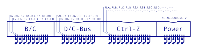
This shows the four right angled boxed headers (identical to the ones used on all the cards so far) - from left to right these are: 8+8 B/C input, 8+8 data bus plus control lines, 10+10 control lines and finally 5+5 power lines. The pins used by the ALU on the control bus are not shown here but effectively take up the second row of pins shown with dashes above. There are also some values here that are used by other cards in the computer that share the same ribbon cable / back plane slots but for the sake of completeness each of the pins are as follows:
- B/C Connector (B + C ALU Input)
- B0-B7 … 8-bit B ALU Input
- C0-C7 … 8-bit C ALU Input
- D/C-Bus (Data Bus + Control Lines)
- D0-D7 … 8-bit Data Bus
- F0-F2 … ALU Function Code (ALU Control Card)
- SN … Sign Condition Register (ALU Control Card)
- CY … Carry Condition Register (as above)
- EZ … Zero Condition Register (as above)
- NZ … Non-Zero Condition Register (as above)
- CL … Condition Register Load (as above)
- Ctrl-Z (Control Line Bus)
- RLA … Register Load A (AD Register Card)
- RLB … Register Load B
- RLC … Register Load C
- RLD … Register Load D (AD Register Card)
- RSA … Register Select A (AD Register Card)
- RSB … Register Select B
- RSC … Register Select C
- RSD … Register Select D (AD Register Card)
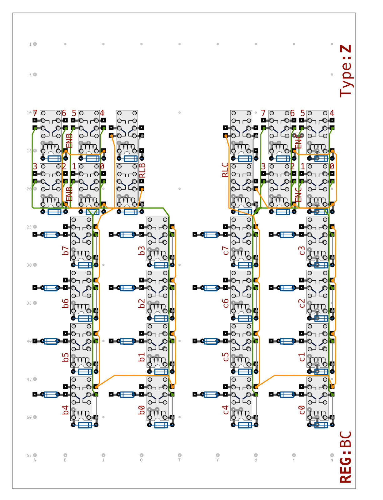
So, finally, wiring everything together we get the following:
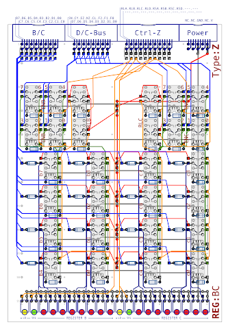
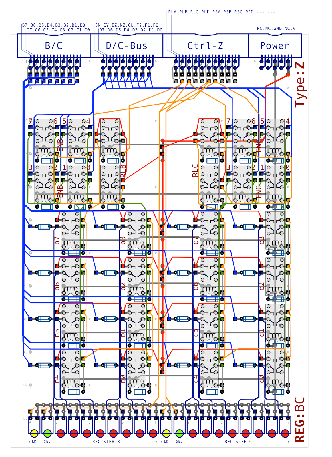
This diagram includes everything mentioned so far along with the power supply and ground lines and all other internal wiring. As with previous cards, the completed BC Register design can be found here in PDF format (so you can zoom right in on the detail). Hopefully the diagram reads OK but if not let me know in the comments.
With the designs for the AD and BC register cards complete I can now get on with some construction. I’ll put the BC card together first as this will then allow me to load the ALU from the data bus rather than directly down the B/C internal bus. Following that I’ll then put the AD card together so that I can store a result from ALU before copying it over to one of the other registers (and so I can then do operations like running addition etc). This time around I’m not going to post quite as heavily during the construction because most of what’s going on is now just repetition of the methods used on the previous cards. That said though I’ll still post anything that seems odd or interesting along the way and I’ll still take plenty of photos throughout construction to dump on you all at a later date.