This post covers the design of a general purpose 8-bit register that can be loaded from the data bus and then selected back to the data bus at a later time. This permits temporary storage of 8-bit values whilst performing various operations, for example, ALU functions. This post goes back over some of the ground already covered by the design of the condition registers which are a slightly simplified version of the registers detailed here.
In the most basic terms we can store a single bit in a relay as follows:
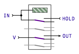
In its initial state the register is off and both the IN and HOLD inputs are off. A value is applied to the IN connection and then the HOLD input is set on and the value at IN removed. If the value was set then the relay would be activated allowing the HOLD input to keep the relay on. The relay will then remain on until the HOLD input is set off. Separately to this power is supplied directly to one of the other relay switches and provides an isolated source of the value held in the relay.
This basic design does need some ‘support’ to gate the input of the relay to ensure that it is only fed to the relay when needed and that the hold line is off when ’loading’ the relay (this also ensures that the hold line can’t back-feed the input line accidentally). Adding these control and gating relays gives us the following:
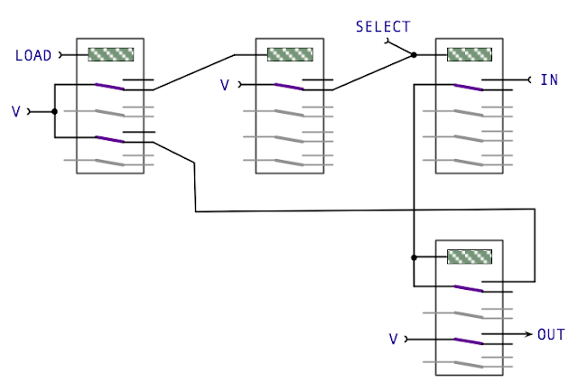
This may look a little over complicated at first but is designed to avoid feedback and oscillation in the control lines (where the relay would turn on and off rapidly turning it into a buzzer … and eventually burn it out). The design for this register is taken from the Harry Porter Relay Computer (and reproduced here with kind permission). There’s a nice explanation on the issue of feedback and oscillation on Harry’s site including the evolution of this design.
One slight issue with this register design is that the data bus must be empty/clear when selecting the value from the register. If any value is present on the data bus then the register will be back fed and effectively take on the logic OR combination of the data bus and register content. Fortunately the sequencer, when designed and built, will ensure that the data bus content is controlled correctly in usual operation but if the registers are operated manually when debugging it’ll be something to watch out for.
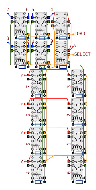
Using the base design above I can modify it to use my DPDT relays and extend to 8 bits:
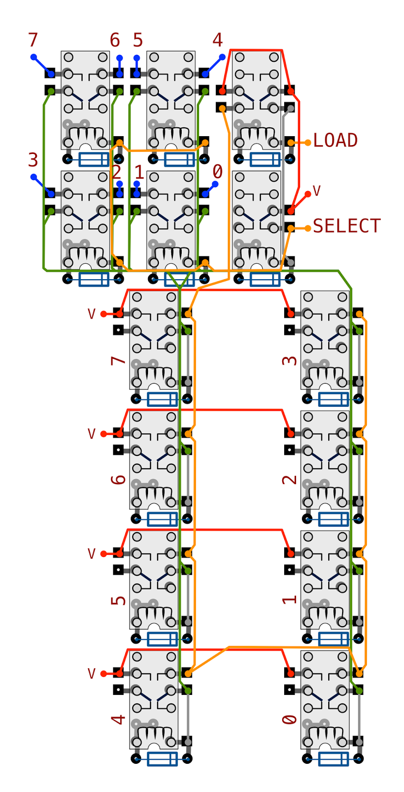
At first glance this looks quite ‘busy’ but breaking it down: the four relays at the top left gate each bit on and off the data bus; the two relays at the top right orchestrate the register load/select operations and finally the eight remaining relays store each of the eight bits. The unconnected pad on each of the lower eight relays will typically be used to drive an LED to show the current status of each register bit. Having this physically isolated from the data bus avoids any back feeding issues.
There’s not really much more to say about the basic register design (hopefully it’s all fairly self explanatory). Using the usual PCB cards I can comfortably fit two 8-bit registers on a single card and so the first registers I’ll produce full designs for will be the following:
- Register B and C
- Register A and D
Each of these is a general purpose register so can be loaded and selected from/to the data bus when needed but B and C additionally drive the inputs to the ALU whilst only registers A and D can be loaded with the result from the ALU. I’ll post the full designs for these two register cards in an upcoming post.