In the last post I introduced the design for the A/D register card (which as its name suggests contains the A and D 8-bit registers). I’m now making a start on the design for the B/C register card and although its pretty much the same as the A/D card there’s an extra complexity because the B/C registers additionally feed the ALU B and C inputs.
For the A and D registers I ended up with the following circuit per 8-bit register:
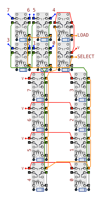
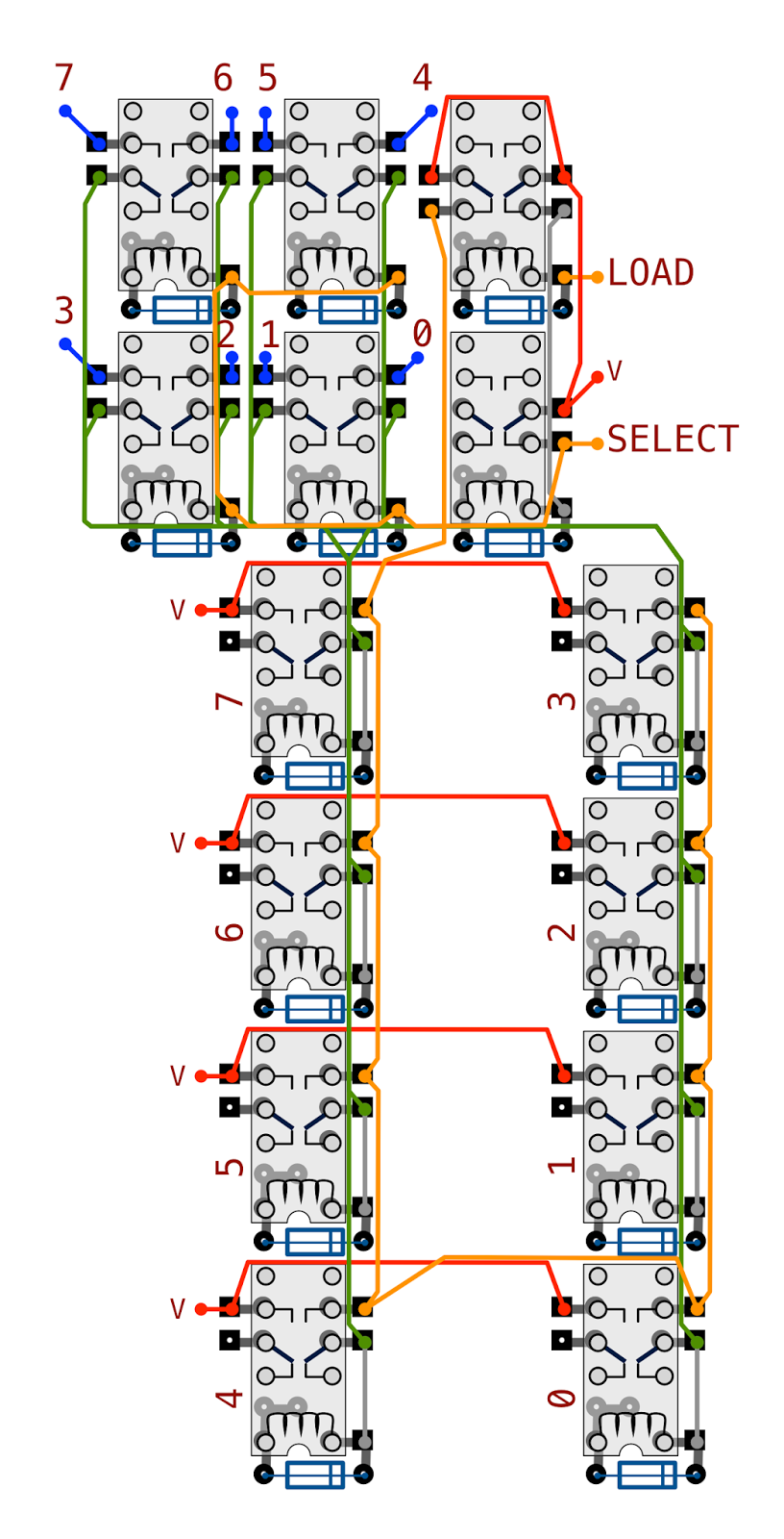
In this design the spare pad on the left of each of the lower relays feeds an LED to show the status of each register bit. This pad is isolated from the register bit circuitry itself by making use of the second DPDT switch on each bit relay. The B and C registers will also need this LED feed but additionally need to provide a permanent feed of the current value in each register bit to the ALU. However, I can’t just piggyback on the pad used to light the LED because there’s a risk that the LEDs could light up in error if anything back feeds up the B or C ALU lines (thereby obscuring the actual value held in the register). A better solution is to isolate the LED feed from the ALU feed however this then requires an extra relay per bit because I’ll then need three DPDT switches rather than the two used above. Diagram wise it’d look like this:
In this design there is now the required two pads available per relay … one for the LED and one for the ALU feed. However, doubling the number of relays also means double the current consumption for each bit that’s holding a value … double the cost in relays … double the soldering … double the frustration etc etc. One way around this would be to stick with the single pad design (with one relay per bit) and place a diode in the feed to the ALU so that back feed cannot occur. This doesn’t come for ‘free’ though and needs some consideration to the effect the diode will have on the ALU feed itself.
The first concern would be the voltage drop across a diode. Assuming a silicon diode is used the voltage drop would typically be 0.7V and so based on a supply of 12V the voltage downstream of the diode would reduce to 11.3V. According to the data sheets for the relays I’m using (the TE/Axicom V23079-A2003-B301) they’ll be happy with anything down to 9V before they’ll refuse to operate so things should be OK here. In fact I could get away with three diodes in series (maybe even four at a push) before I’d run in to problems.
With the first concern ticked off the next one would be over the current flowing through the diode. Each of the relays I’m using consumes around 11mA whilst the coil is energised (based on a 12V supply and a coil resistance of 1029 ohms … assuming I’ve followed ohms law correctly of course ;). A typical signal diode like the 1N4001 can pass up to 100mA before it’ll get a sweat on so in theory I could feed 9 relays through the diode without problems. This point actually raises a greater issue which I always have in the back of mind when designing the various parts of this computer … fan out.
Fan out (in the design of this computer at least) is a measure of how many relays I can drive from a single output of a single relay switch (assuming that switch is fed directly by the power source as it is in the above diagrams). The voltage in this case isn’t so much of a concern because relays in parallel will receive the same voltage but the current of multiple relays will add up and could cause issues. Actually, my worry about the max diode current is actually second place to the amount of current the wire wrap wire itself is happy passing. This ‘Kynar’ wire is gauged at 30AWG and I’m working on the basis that it can carry around 100mA (as a conservative estimate). Converting that 100mA to my preferred currency comes out at 9 relays. Because of this limit I’ve always got a 9 relay fan out limit in my head to keep things within limits and in practice most individual outputs wouldn’t feed more than a couple of outputs at a time. When manually operating the computer it could be possible to do something silly (like load multiple registers off the data bus simultaneously) but even then I’m pretty sure things would be within limits. Fortunately if I do find anywhere is getting a bit ‘hot’ design wise I can always lay down multiple wire wraps between two points to increase the current carrying capacity.
Anyho, that’s settled, I’ll use a diode to keep the feeds isolated and therefore I can use the same ‘one relay per bit’ design used in the A and D registers. I’ll put together a full schematic for the B and C registers now and then post them up here in due course. Incidentally, in other news my laser cutting has been dispatched so should be with me in the next couple of days so I’m not going to be able to resist putting that together and posting about it so it’ll probably be an enclosure post next followed by a register post.