In the last post I introduced the design for a general purpose 8-bit register. This post covers taking two of those registers along with status LEDs and gating relays to implement the full A and D registers.
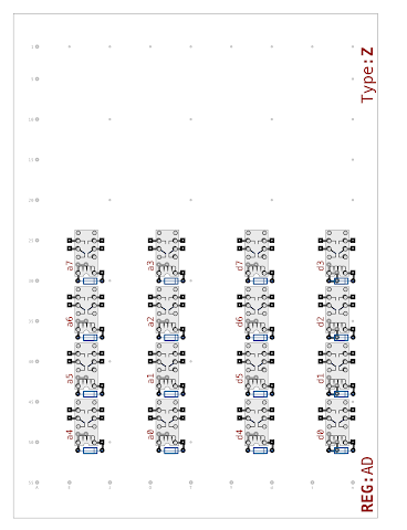
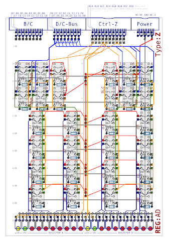
So, diving straight in, here is what the main bit relays look like for the two 8-bit registers when placed on the usual 55 x 40 hole pad board (excluding wire links):
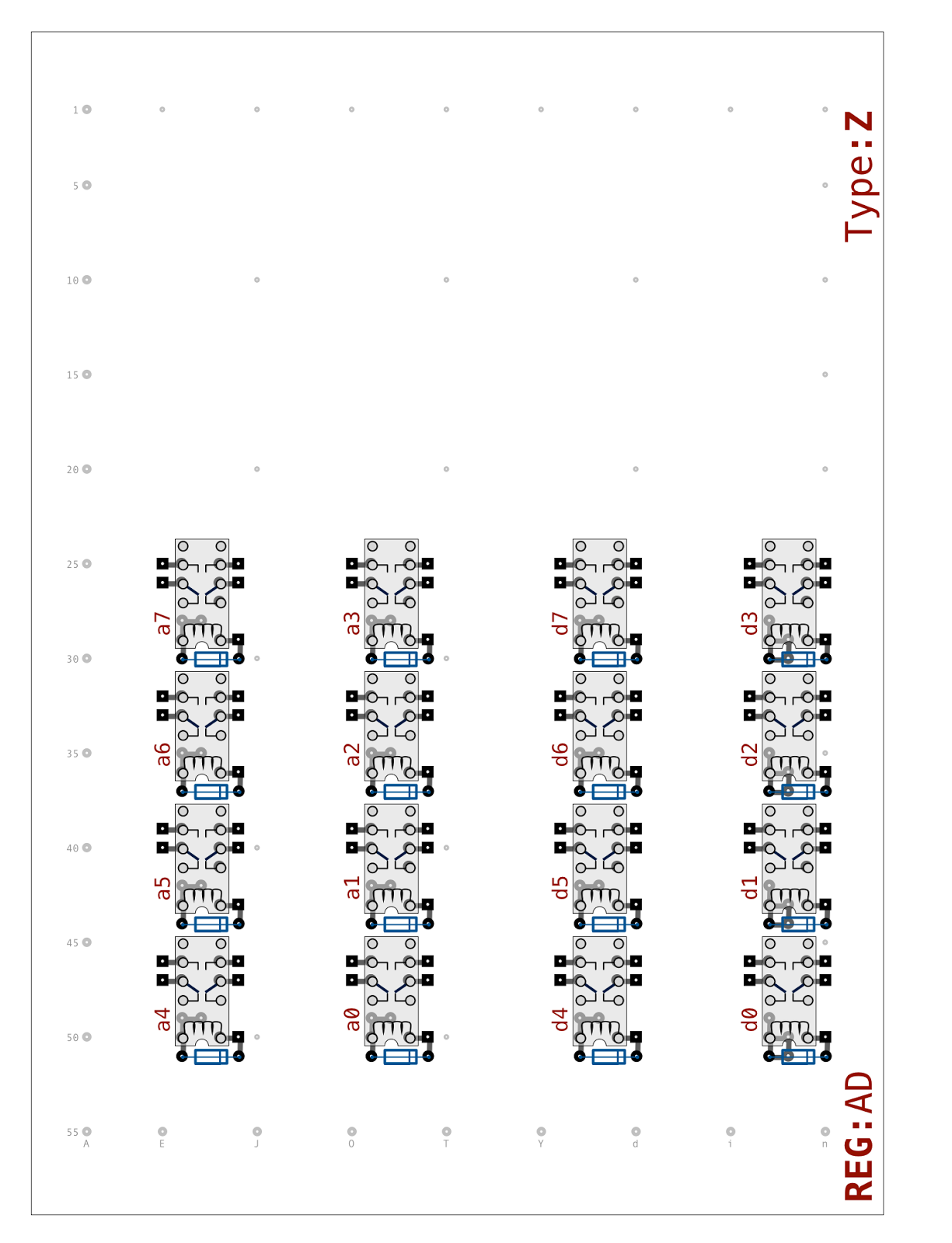
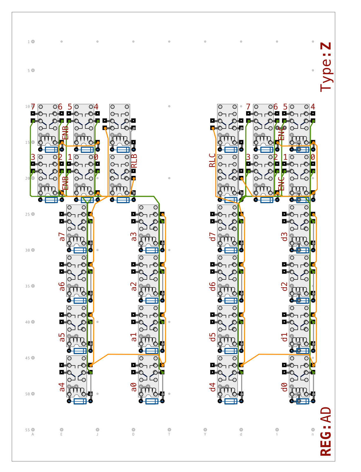
Each of the relays above stores a single 1-bit value so there’s 16-bits worth in total (which could all be used together if we were making a 16-bit register) or two lots of 8-bits (for our two 8-bit registers). Each of the 1-bit register relays need gating to and from the data bus so that the values stored don’t conflict with any other value on the data bus. With these additional control and gating relays added we get the following (this time including internal wire links in the 1-bit register relays and result links between the 1-bit register relays and the gating relays):
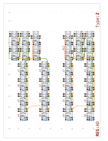
So, that’s it for relays on this card. As with previous cards I’d like to be able to display the current value being stored in the registers regardless of the whether that value is being gated on to the data bus or not. This allows me to confirm correct operation and test/debug the card independently. For this 20 LEDs are needed … 8 for each of the two 8-bit register values, 2 to show when each register is being loaded and finally 2 for when each register is being gated on to the data bus (selected). Fortunately there’s just enough room down the front of the card to fit in the 20 LEDs required in single row LED holders and so this also simplifies the wiring behind the LEDs. The LEDs are, as always, the same 12V ones used in all the previous cards (with an integral resister). Colour wise I’m continuing with the theme of red for a bit value, yellow for inputs or control signals and green for output control signals or state. Diagram wise then it looks like this:
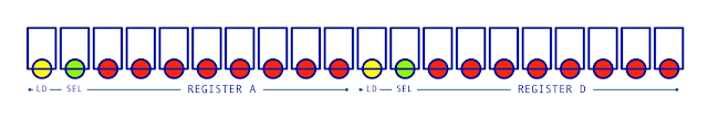
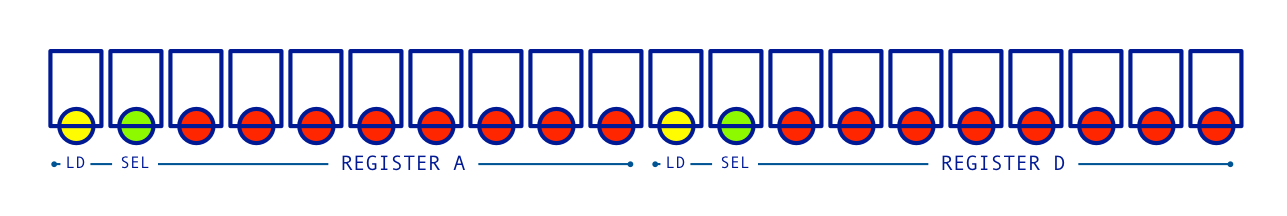
Each block in the diagram represents a single 3mm LED in a plastic holder. Each LEDs is pushed into the holder from the front and the pair of LED legs are bent at 90 degrees.
Next up is the connections to other parts of the computer. There is the 8-bit data bus, power connections and finally the control signals to load/select the A and D registers. This isn’t too far away from the layout used by the ALU cards and so by keeping with the same connector lines a ribbon cable can be passed through all the sockets (or rather I can use the backplane card) to connect several cards together. The diagram of the connectors look like this:
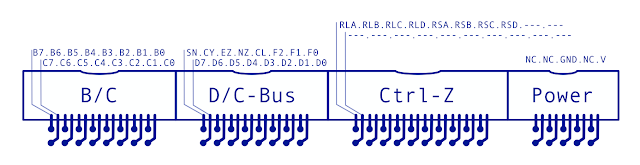
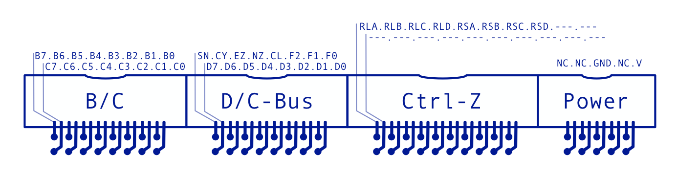
This shows the four right angled boxed headers (identical to the ones used on all the ALU cards) - from left to right these are: 8+8 B/C input, 8+8 data bus plus control lines, 10+10 control lines and finally 5+5 power lines. The pins used by the ALU on the control bus are not shown here but effectively take up the second row of pins shown with dashes above. There are also some values here that will be used by other cards in the computer that share the same ribbon cable / back plane slots but for the sake of completeness each of the pins are as follows:
- B/C Connector (B + C ALU Input)
- B0-B7 … 8-bit B ALU Input
- C0-C7 … 8-bit C ALU Input
- D/C-Bus (Data Bus + Control Lines)
- D0-D7 … 8-bit Data Bus
- F0-F2 … ALU Function Code (ALU Control Card)
- SN … Sign Condition Register (ALU Control Card)
- CY … Carry Condition Register (as above)
- EZ … Zero Condition Register (as above)
- NZ … Non-Zero Condition Register (as above)
- CL … Condition Register Load (as above)
- Ctrl-Z (Control Line Bus)
- RLA … Register Load A
- RLB … Register Load B (BC Register Card [to be covered in a later post])
- RLC … Register Load C (as above)
- RLD … Register Load D
- RSA … Register Select A
- RSB … Register Select B (BC Register Card [to be covered in a later post])
- RSC … Register Select C (as above)
- RSD … Register Select D
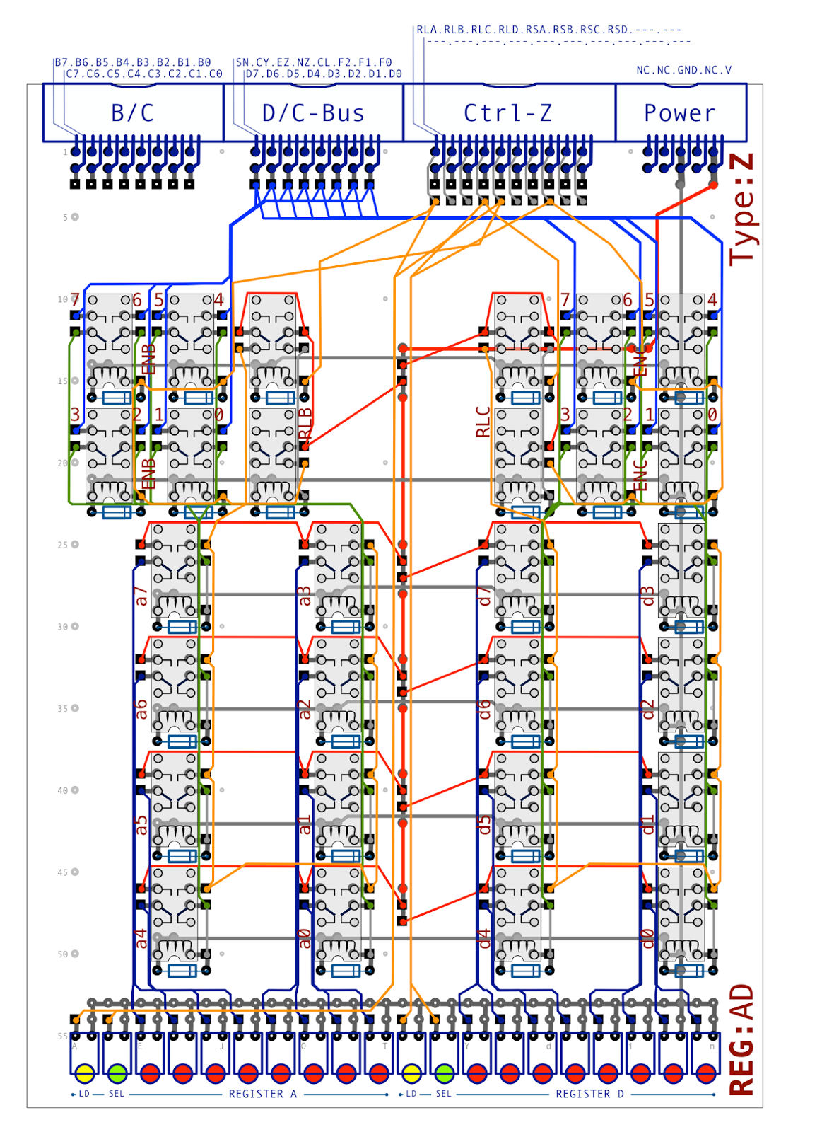
So, finally, wiring everything together we get the following:
This diagram includes everything mentioned so far along with the power supply and ground lines and all other internal wiring. As with previous cards, the completed AD Register design can be found here in PDF format (so you can zoom in and out as you wish). Hopefully the diagram reads OK but if not let me know in the comments.
In the next post, assuming my laser cut enclosure parts don’t arrive first in which case I’ll post about those next, I’ll cover the design of the BC register which is very similar to this one but has the additional complexity of directly feeding the ALU via the B/C bus.