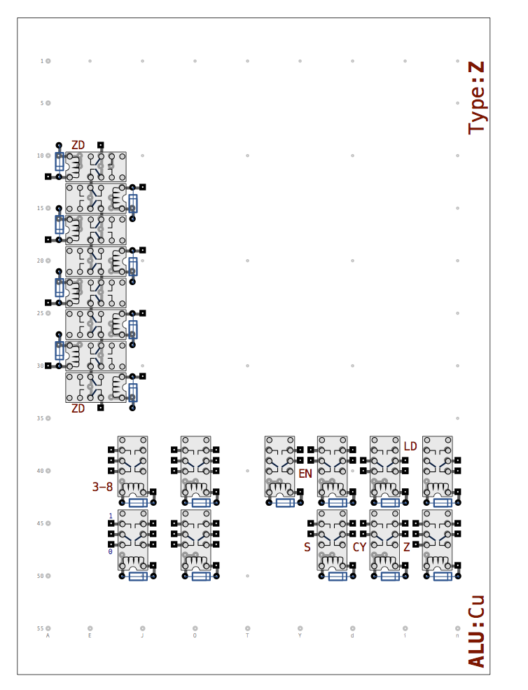
In the last three posts I introduced the design for the 3-to-8 Function Decoder, Zero Detect circuit and the Condition Registers. In this post I’ll put all three of these components together to make up the ALU Control Card. So, placing the relays from the three components onto the card (excluding wire links) we get the following:

Unlike the other cards that make up the full ALU (the logic and arithmetic cards) things aren’t quite so tightly packed in this time. Despite this I’ve pushed the relays out towards the edges of the card to leave room for any future ALU control expansion or modifications without requiring an extra card. I’ll be displaying the current state of the 3-to-8 Decoder and Condition Registers with LEDs along the front of the card as with the other cards designed so far. The LEDs are the same 12V ones as before (to save space that would be used by the additional resistors) and follow the same colour code of red for results, yellow for inputs and green for output control signals. Diagram wise the display looks like this:
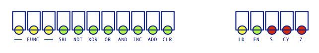
Each block in the diagram represents the same 3mm LED in a plastic holder as before (with the LED pushed into the holder from the front and the LED legs bent at 90 degrees). The left hand LEDs relate to the 3-to-8 Decoder (3-bit function code followed by the derived 8 control lines) and the right hand ones to the Condition Registers (Register Load and Enable followed by Sign, Carry and Zero Register values).
Connector wise things are similar to the Logic and Arithmetic card: there is the 8-bit data bus, power connections and control signals but the 8-bit inputs B and C are not required for this card. The diagram of the connectors look like this:
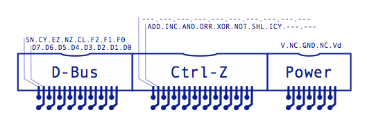
This shows the three right angled boxed headers (as per the Logic and Arithmetic card) — from left to right these are: 8+8 data bus plus control lines, 10+10 control lines and finally 5+5 power lines. Again, some of these connection lines are used by other cards that share the same ribbon cable / back plane slots but for the sake of completeness each of the pins are as follows:
- D-Bus (Data Bus + Control Lines)
- D0-D7 … 8-bit Data Bus
- F0-F2 … ALU Function Code (used by the 3-to-8 Function Decoder on this card)
- SN … Sign Condition Register (produced by this card)
- CY … Carry Condition Register (as above)
- EZ … Zero Condition Register (as above)
- NZ … Non-Zero Condition Register (as above)
- CL … Condition Register Load (as above)
- Ctrl-Z (Control Line Bus)
- ADD … ALU Add Output Enable (produced by this card)
- INC … ALU Increment Output Enable (as above)
- AND … ALU AND Output Enable (as above)
- ORR … ALU OR Output Enable (as above)
- XOR … ALU XOR Output Enable (as above)
- NOT … ALU NOT Output Enable (as above)
- SHL … ALU Shift Left Output Enable (as above)
- ICY … ALU Internal Carry Result (used by this card)
So, with everything together including all the wiring, power supply and ground lines we get the following:

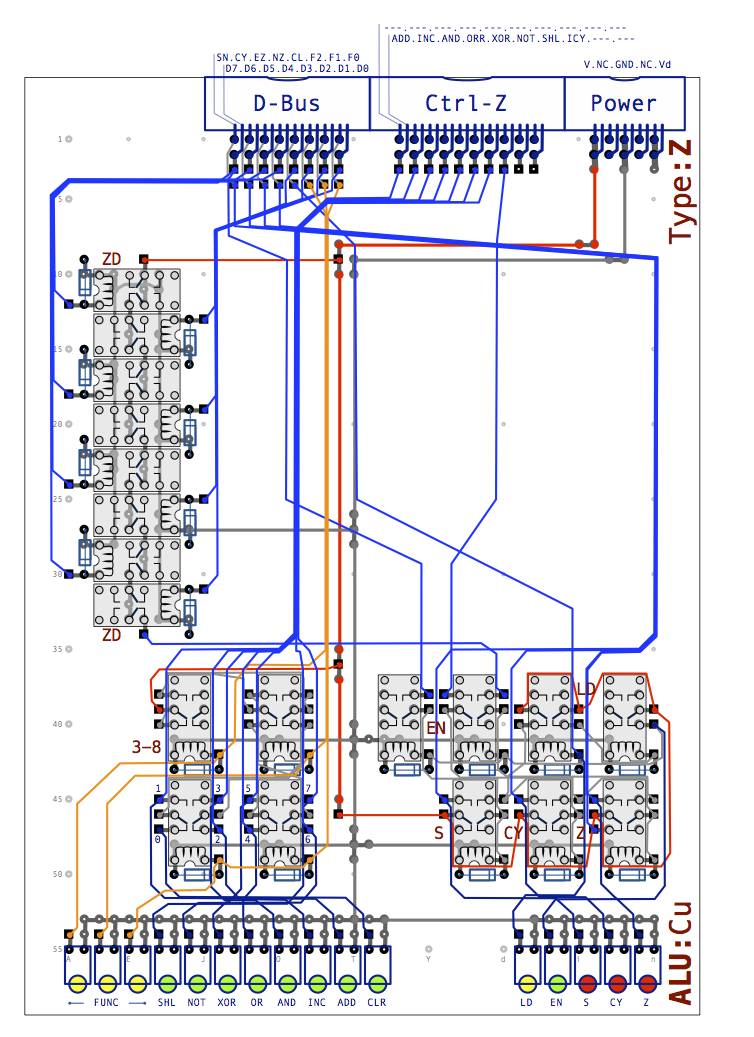
As before in previous posts the completed Arithmetic Control Card design can be found here in PDF format (so you can zoom in for more detail).
With the three cards that make up the complete ALU all designed and ready to go I think it’s finally time to actually start some construction and take a break from creating all these diagrams. This will allow me to actually try out some of the theory and to refine the construction methods but does carry the risk that I make something that’s incompatible with the rest of the computer design. However, I’ve got the registers worked out in my head and, of course, I’m basing my design on the Harry Porter Relay Computer so I’m confident enough now to get the soldering iron out.