In the last post I introduced the design for a 1-bit Logic Unit. This post covers the design effort to cram 8 of these on to a single pad board complete with connectors, status LEDs and gating relays thereby forming a complete 8-bit Logic Unit.
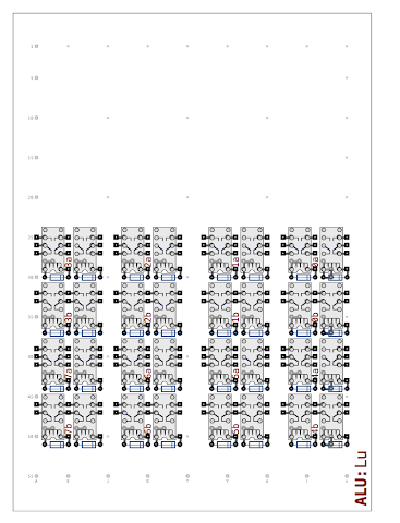
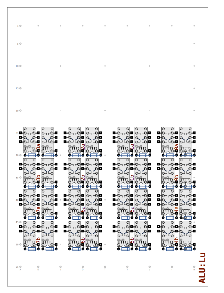
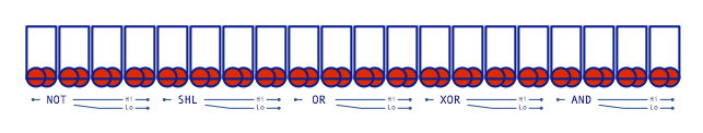
Sticking with the same diagram style I introduced in the last post here is what 8 of the 1-bit Logic Units look like all crammed on to the 55 x 40 hole pad board (excluding wire links):
Things are a bit tight but as I often find when using these pad boards things magically seem to fit after trying a couple of permutations … it’s almost like the pad boards were designed with this sort of thing in mind ;)
Each of the 1-bit Logic Unit produces five results simultaneously (AND, OR, XOR, NOT and SHL) but only one of these can be selected/gated back on to the data bus at a time and so gating relays are needed. Each result requires 4 relays for a total of 8 switches to gate the 8 bits of the result. With these additional relays added we get the following (this time including internal wire links in the 1-bit Logic Units and result links between the Logic Units and the gating relays):
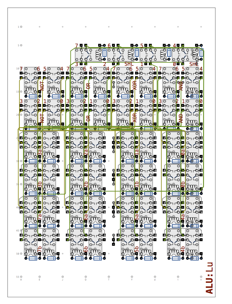
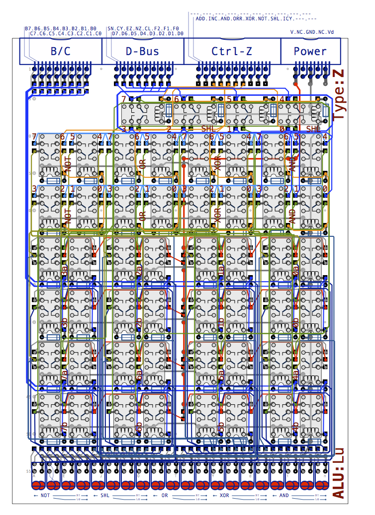
Things are getting a little busier now but that’s it, thankfully, for relays on this board. The next thing I want to be able to do is display the five results that are being generated by each 1-bit Logic Unit regardless of the result that is being gated on to the data bus — this way I will be able to easily confirm correct operation given a known input. This means a total of forty LEDs (8 LEDs for the 8-bits of each of the five results). As there are 40 holes available across the board that’s room for a maximum of 20 LEDs — half as many needed — therefore two rows of LEDs will be required. Also, regular 5mm LEDs are going to be too big to comfortably sit side by side so I’ll drop down to 3mm LEDs instead. One thing I have been thinking about is that it’d be nice to have the LEDs at a right angle to the board so they can be viewed from the front when the board is laying flat. Now, one thing the LEDs will need are resistors to limit the current however that will take up even more room and would be complex to wire/solder in so I’ve selected a range of 12V LEDs that have an integral resistor — these are more expensive than regular LEDs (relatively) but vastly simplify things construction wise. Because of having to cram the LEDs in I’ll split the bottom row of 20 in to five sets of the lowest bits from each result and the top 20 in to five sets of the highest bits. Diagram wise it looks like this:
Each block in the diagram represents two 3mm LEDs stacked vertically in a plastic holder. The LEDs are pushed into the holder from the front and then the pair of LEDs legs are bent at 90 degrees.
Next up is the connections to other parts of the computer. There is the two 8-bit inputs B and C, the 8-bit data bus, power connections and finally the control signals to select which result should be gated on to the data bus. For these I’m using right angled boxed headers for a connection to a ribbon cable although I have it in mind to use another pad board as a backbone for connecting several cards together (more on this in a later post). The diagram of the connectors look like this:
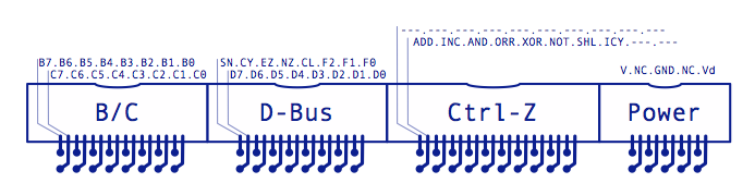
This shows four right angled boxed headers — from left to right these are: 8+8 B/C input, 8+8 data bus plus control lines, 10+10 control lines and finally 5+5 power lines. There are some values here that will be used by other cards in the computer that share the same ribbon cable / back plane slots but for the sake of completeness each of the pins are as follows:
- B/C Connector (B + C ALU Input)
- B0-B7 … 8-bit B ALU Input
- C0-C7 … 8-bit C ALU Input
- D-Bus (Data Bus + Control Lines)
- D0-D7 … 8-bit Data Bus
- F0-F2 … ALU Function Code (ALU Control Card [to be covered in a later post])
- SN … Sign Condition Register (ALU Control Card [to be covered in a later post])
- CY … Carry Condition Register (as above)
- EZ … Zero Condition Register (as above)
- NZ … Non-Zero Condition Register (as above)
- CL … Condition Register Load (as above)
- Ctrl-Z (Control Line Bus)
- ADD … ALU Add Output Enable
- INC … ALU Increment Output Enable
- AND … ALU AND Output Enable
- ORR … ALU OR Output Enable
- XOR … ALU XOR Output Enable
- NOT … ALU NOT Output Enable
- SHL … ALU Shift Left Output Enable
- ICY … ALU Internal Carry Result (ALU Arithmetic Card [to be covered in a later post])
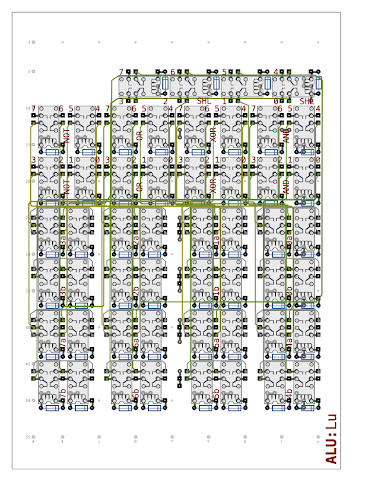
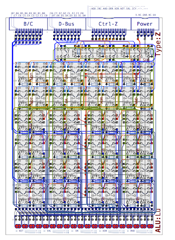
So, wiring everything together we get the following assault on the eyes:
To make things a bit easier to see the completed Logic Unit design can be found here in PDF format (so you can zoom in/out to your hearts content). Hopefully the diagram shouldn’t need too much more explanation (although let me know in the comments if that’s not the case) as it’s just wires from connectors to relays, relays to connectors, relays to LEDs and power everywhere else.
In the next post I’ll cover the design of a 1-bit adder which will then lead on to the 8-bit Arithmetic Unit which, with the Logic Unit here, makes up two-thirds of the whole ALU design.