In the last post I introduced the design for the 1-bit Arithmetic Unit. This post covers connecting eight of these units together to make an 8-bit Arithmetic Unit along with result gating and increment functionality.
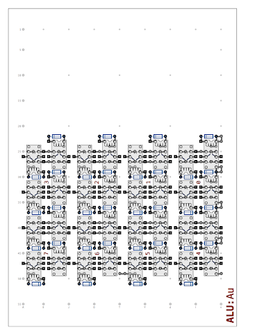
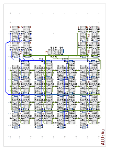
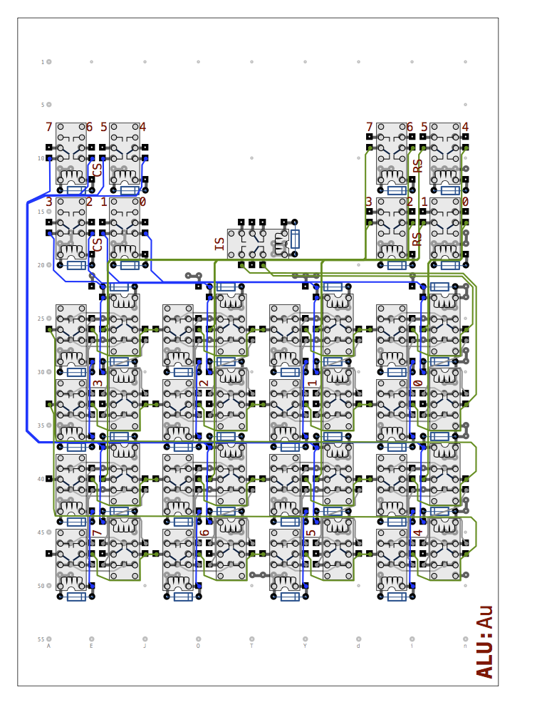
So, diving straight in, here is what eight of the 1-bit Arithmetic Units look like all together on the usual 55 x 40 hole pad board (excluding wire lines):
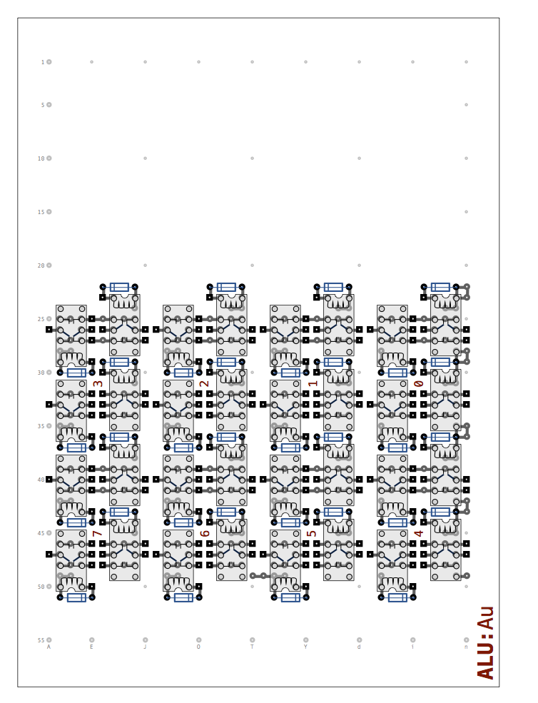
As before (with the Logic Unit card) things are a bit on the tight side but everything fits within the 40 hole horizontal confines of the pad board (as if by magic). Each of the 1-bit Arithmetic Units produces a 1-bit output and these need gating back on to the data bus so that the result doesn’t conflict with any other Logic Unit output (or any future outputs from places like the Registers etc). With these additional relays added we get the following (this time including internal wire links in the 1-bit Arithmetic Units and result links between the Arithmetic Units and the gating relays):
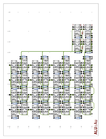
This would now be enough relays to handle adding to 8-bit numbers together however the Arithmetic Unit has two modes: Add and Increment. The increment function adds one to the B input and so to make this work with the existing design we need to disconnect the C input when incrementing and set the carry in bit (to act as the +1). With the C input gating relays and the carry in relay we get the following:
So, that’s it for relays on this card — slightly less than on the Logic Unit card but still quite densely packed in there (and all on a 0.1 inch pitch so it’ll still be a fiddly construction too). As with the Logic Card I’d like to be able to display the current result being generated regardless of the whether that result is being gated on to the data bus — again, this allows me to confirm correct operation and test/debug the card independently. This time around only 10 LEDs are needed … 8 for the 8-bit result, 1 for the carry in line and 1 for the carry out line. As there’s a lot more room to play with than before I can get away with using single row LED holders and so this also simplifies the wiring behind the LEDs as there’s only two legs rather than four per holder. The LEDs are the same 12V ones used in the Logic Unit Card (to spare the need for a separate resistor) but I introduce green and yellow ones this time. Generally I’ve decided to use red for a bit result, yellow for inputs or control signals and green for output control signals or state. Diagram wise then it looks like this:
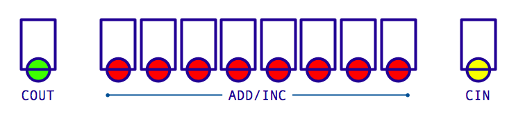
Each block in the diagram represents a single 3mm LED in a plastic holder. A LEDs is pushed into the holder from the front and the pair of LED legs are bent at 90 degrees.
Next up is the connections to other parts of the computer. There is the two 8-bit inputs B and C, the 8-bit data bus, power connections and finally the control signals to select whether the unit is adding or incrementing. This is the same layout that the Logic Unit uses so that ribbon cable can be passed through all the sockets (or I can use another pad board as a backbone for connecting several cards together). The diagram of the connectors look like this:
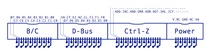
This shows the four right angled boxed headers (identical to the ones used on the Logic Unit) - from left to right these are: 8+8 B/C input, 8+8 data bus plus control lines, 10+10 control lines and finally 5+5 power lines. There are some values here that will be used by other cards in the computer that share the same ribbon cable / back plane slots but for the sake of completeness each of the pins are as follows:
- B/C Connector (B + C ALU Input)
- B0-B7 … 8-bit B ALU Input
- C0-C7 … 8-bit C ALU Input
- D-Bus (Data Bus + Control Lines)
- D0-D7 … 8-bit Data Bus
- F0-F2 … ALU Function Code (ALU Control Card [to be covered in a later post])
- SN … Sign Condition Register (ALU Control Card [to be covered in a later post])
- CY … Carry Condition Register (as above)
- EZ … Zero Condition Register (as above)
- NZ … Non-Zero Condition Register (as above)
- CL … Condition Register Load (as above)
- Ctrl-Z (Control Line Bus)
- ADD … ALU Add Output Enable
- INC … ALU Increment Output Enable
- AND … ALU AND Output Enable
- ORR … ALU OR Output Enable
- XOR … ALU XOR Output Enable
- NOT … ALU NOT Output Enable
- SHL … ALU Shift Left Output Enable
- ICY … ALU Internal Carry Result (produced by this card)
The last signal there (ICY) is produced by the last 1-bit Arithmetic Unit’s Carry Out signal and is passed down the Control Bus back to the Control Card where it can be used to set the Carry Condition Register. This differs to the CY signal on the Data Bus which is the output from the Carry Condition Register itself.
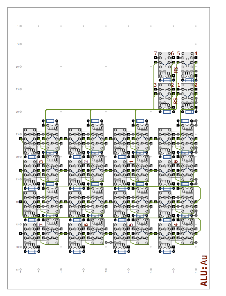
So, finally, wiring everything together we get the following jumble:
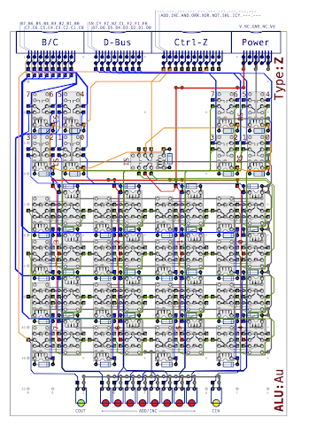
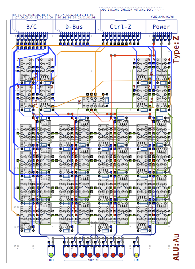
This diagram includes everything mentioned so far along with the power supply and ground lines and all other internal wiring. As before, the completed Arithmetic Unit design can be found here in PDF format (so you can zoom in and out as you wish). Hopefully the diagram reads OK but if not let me know in the comments.
In the next post I’ll cover the final parts of the ALU: the zero detect circuit, the function decoder and the condition registers … the three of these combining to form the final ALU Card: the Control Unit.