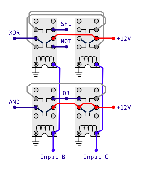
This post covers the design of a 1-bit Logic Unit that can produce AND, OR, XOR, NOT and SHL (Shift Left) outputs from two input bits B and C. Here’s a schematic of the 1-bit Logic Unit (based directly on the one used in the Harry Porter Relay Computer):
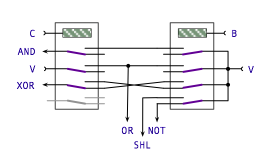
The diagram shows two 4PDT (4 pole double toggle) relays with the coils of each shown as a striped box at the top. The four double toggle switches are also shown on each relay and the current position of each switch is as when the relay is off. When power is applied to the relay coil all four switches change over simultaneously. The two relays together with all the various connections form the 1-bit Logic Unit. Inputs to the unit are shown with ‘cupped’ line ends: B and C are the two 1-bit inputs; V is a permanent connection to the power supply. Outputs from the unit are shown with an arrowed line end: the outputs AND, OR, XOR, NOT and SHL. Wire joins are shown with a dot (otherwise the wire is passing over but not connecting to another wire) and unused switches on a relay are shown in grey.
The design itself is pretty much self explanatory (hopefully) … just follow the wires through the switches to get to the result. For example, following the V (voltage/power) input on the right … if the B input is on then you can get through the top switch over to the left relay — if the C input is also on then you can get through to the AND output — therefore, if both B and C are on then power is supplied to the AND output. Note that SHL would be treated as the bit 2 output for the bit 1 input as essentially all this unit does is sets SHL on when input B is on and off when B is off. Another thing worth noting about this design is that it may appear, at first glance, to be using more relay switches than necessary but is designed this way to avoid any ‘backfeed’ on one of the outputs affecting one of the other results.
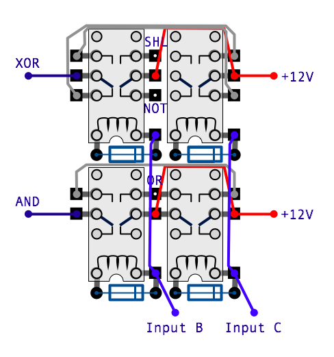
As mentioned in my last post I’ll be using the smaller DPDT (double pole double toggle) relays in my computer and so I’ll need to double up the number of relays to counter the halving of the number of poles — I can therefore transform the above diagram to the following:

This is the second diagram style I’ll be using on this blog. Each relay is a direct scaled representation of the DPDT TE Connectivity relay I specified in my last post and, again, the switch positions shown in each relay is for when the relay is off. The coils in this particular relay model are polarised and so have positive and negative pins — in this diagram the ground is shown on the left and the input (positive/power) is shown on the right of the coil.
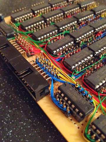
Now, diagrams are all very well but it’s now time to start thinking about how this translates into a physical form … and I’ve got a bit of an admission to make … this isn’t my first go at making an ALU … I constructed a fully working 8-bit ALU last year based on CMOS NAND gates so I’ve already pretty much got a construction method that suits me, one that’s tried and tested (albeit a bit unconventional). The base for my construction is pad board which I’ve used many times for prototyping in the past and found it works well for me. The one I use is from bitsbox and is 160 x 115 mm featuring 55 x 40 holes on a 0.1 inch pitch. The challenge for me in this project is fitting everything around these boards … and with the 8-bit logic unit it’s going to be quite a squeeze (more on that later). Ideally I want to use a socket of some kind for the relays rather than solder them directly so it’s easier to switch out defective relays (removing anything that has multiple pins when it’s been soldered can be an absolute pain) but I’ll look into that later.
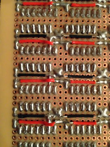
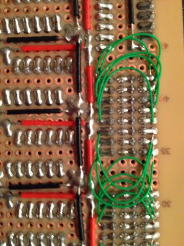
I’ll be doing the same for the ground rails this time around but the power connections will go top side as they aren’t as regular as they are for supplying ICs. Speaking of the top side of the board I chose to use wire wrap as it allowed me to easily make modifications (or rather, to correct mistakes easily). However, I discovered that wire wrapping posts are really expensive so I tried using header pins and found they worked OK. This could definitely be considered as an unconventional construction technique again but seems to work well … the only problem is that due to the height of the header pins there’s a limit of two wire wraps per pin (my design always allows for this). The resulting wire wraps look like this:
Quite pretty (well, at least I think so ;) Anyway, going back to the earlier diagram we can thereby convert:
into:
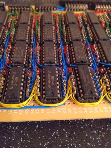
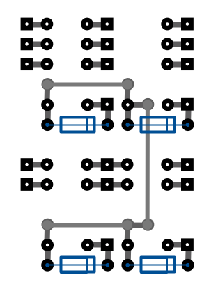
This diagram shows the header pins alongside each relay (black squares) linked with solder where appropriate to the relay pins (thick grey lines). The wire wrapped wire links are shown in various colours (light blue for inputs, dark blue for outputs, red for power supply and grey for internal links). Also shown immediately below each relay coil is a flyback diode to handle the voltage spike created when the relay turns off and the coil’s magnetic field collapses. Here is the same diagram with relays and connections omitted and with partial ground rail shown:
… and that about wraps it up for the basic 1-bit Logic Unit. In the next post I’ll cover taking 8 of these units and cramming them on to a single pad board along with intermediate result LEDs and gating relays (to place a selected result back on to the data bus).