This post covers the design of a 1-bit Arithmetic Unit that can add two input bits together (B and C) with carry in and out. Here’s a schematic of the 1-bit Arithmetic Unit (based directly on the one used in the Harry Porter Relay Computer):
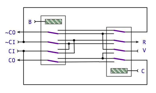
The diagram shows two 4PDT relays (just as before for the 1-bit Logic Unit) but this time the second relay has been rotated 180 degrees to make the diagram simpler to draw. B and C are the two 1-bit inputs that drive the relay coils, V is a permanent connection to the power supply and R is the resulting bit. CI is the carry in signal along with its inverted partner ~CI. Similarly CO is the carry output and ~CO is its inverted partner. It’s the use of these regular and inverted carry signals that makes this design so neat … and actually this isn’t one of Harry’s … this design goes back a lot further.
This full adder circuit was actually invented by Konrad Zuse for his Z3 computer. The Z3 was also built out of relays just like the computer I’m building however he completed his first … by quite some way … back in 1941 … in wartime Berlin. I think it’s fair to say that Zuse’s machine could be considered the first functional computer (as all previous ‘computers’ were mechanical calculators) and the efficiency of this design is quite impressive — using the ‘dual rail’ carry lines to cut down on the switch count and to keep everything within two relays. There’s a simulation of this circuit if you’d like to see an interactive version of this circuit rather than staring at a dry old diagram.
As always, this 4PDT design is fine for those with 4PDT relays … I’m using the smaller DPDT ones so I’ll need to double up the relay count. I therefore transform the above diagram to the following:
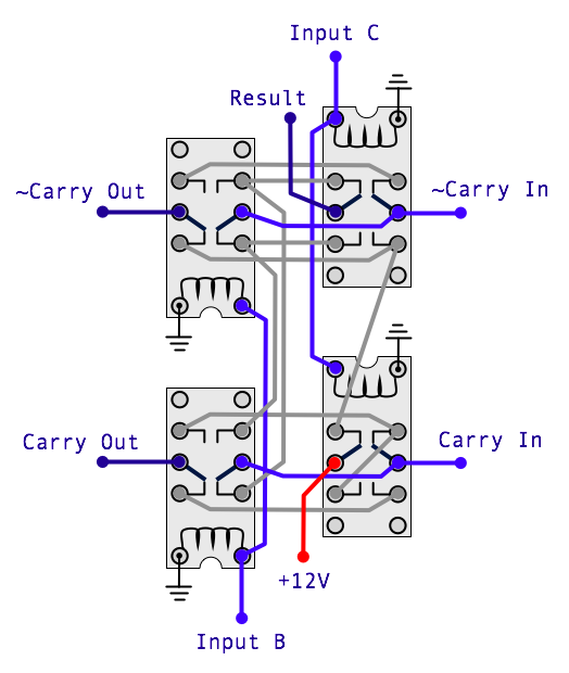
So, certainly not as nice to look at as the 4PDT version but with the
equivalent functionality nonetheless. This layout focusses on lining up the
carry in and outs so that each unit can be stacked alongside the next one but
at the cost of a few ugly link wires. To make things simpler when
constructing the full 8-bit Arithmetic Unit I’ll run the parallel links
between the outer switches of the relays on the solder side of the pad board
with soldered link wire and the parallel links between the top inner relay
switches with solder links or perhaps a jumper to bridge the two header pins.
All the other links will be wire wrap as usual. In summary then, it’ll take
the physical form as follows:
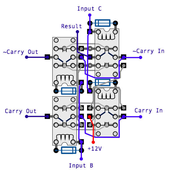
… and here’s the same diagram with relays and wires (on the component side of the pad board) omitted and with partial ground rails added …
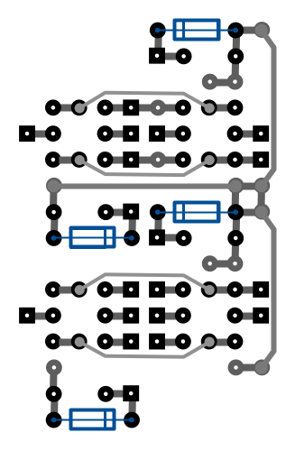
That’s it for the 1-bit Arithmetic Unit. In the next post I’ll cover linking 8 of these units together, gating the result and handling the increment function.